Original Documentation... |
|
Article
Date: |
November, 1999 |
Magazine
Volume: |
5 |
Issue: |
11 |
Author(s): |
|
Debugging
logic in BGA packages can be problematic |
|
Until now,
successive generations of chip packages
have kept pace with the relentless increase
in chip gate counts. Ever increasing interconnect
density and speed have forced the transition
from Dual Inline Packages (DIPs), Plastic
Leadless Chip Carriers (PLCCs), and Quad
Flat Packs (QFPs) to ball-grid array (BGA)
packaging. This transition to BGA packaging
creates problems for manufacturing, test,
and debug. Debug issues, in particular,
arise because device pins are literally
buried underneath the package. Traditional
techniques for probing and inspecting pins
cease to work when pins are no longer accessible.
|
|
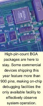
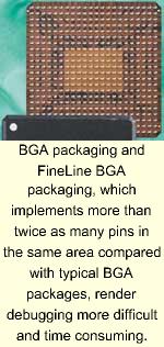
QFP packages,
with exposed pins around the periphery,
become prohibitively large above a 250-pin
count. A 304-pin RQFP package takes up 2.8
in.2 of board space, nearly six times as
much as the 0.5 in.2 occupied by a 324-pin
Fine-Line BGA. Continuing the trend, commercial
devices shipping this year feature more
than 900 pins. As a result, BGA packages
and buried pins are here to stay. |
|
 Manufacturing
techniques evolved rapidly to test and verify
boards incorporating BGA packages. The JTAG
boundary-scan standard, for example, provides
a satisfactory solution for verifying correct
electrical connection to every pin, and
most high-pin-count ASICs incorporate a
four-pin JTAG test-access port and boundary-scan
capabilities. Various x-ray techniques exist
that verify solder integrity-allowing for
good old-fashioned (and surprisingly accurate)
visual inspection, even when pins can't
be seen. Manufacturing
techniques evolved rapidly to test and verify
boards incorporating BGA packages. The JTAG
boundary-scan standard, for example, provides
a satisfactory solution for verifying correct
electrical connection to every pin, and
most high-pin-count ASICs incorporate a
four-pin JTAG test-access port and boundary-scan
capabilities. Various x-ray techniques exist
that verify solder integrity-allowing for
good old-fashioned (and surprisingly accurate)
visual inspection, even when pins can't
be seen.
Manufacturing boards with
fully tested chips based on a verified design
are one thing - debugging a design-in-process
is another. "System debug" is
often the longest bar in a product development
schedule. And debugging is rendered all
the more difficult and time consuming when
many signals are buried beneath BGA packages. |
|
Traditional
debugging tools |
The principal
tools for debugging digital hardware are
the oscilloscope and logic analyzer. A modern
oscilloscope used by a young engineer today
may have many advanced features, but it's
still recognizable as a descendent of the
scope used by his or her grandfather 50
years ago. Both scopes and analyzers implicitly
assume that signals are accessible somewhere
on an exposed metal trace. With ever increasing
levels of integration, more and more signals
are disappearing inside the package. And
now, with the advent of BGA packages, even
package pins themselves cannot be probed.
|
|
 Chip
pins have always given engineers something
to look at when debugging their systems.
On boards full of SSI logic, an engineer
could literally trace a problem back through
logic, gate-by-gate, with just an oscilloscope
probe, and find a problem's origin. Even
with high-gate-count chips, a great deal
of debugging is accomplished just by probing
inputs and outputs. But with BGA packages,
there's often, literally, no place to hang
a scope probe. Although some device pins
can be connected to pc-board test points,
this is only practical for a small minority
of the pins on a large BGA device. Test
points are obviously useful, and traditional
scopes and logic analyzers will be with
us a long time. But naturally, test points
usually represent signals that a logic designer
expects to look at. And bugs, by their very
nature, inevitably arise where you don't
expect them. So, more frequently, you're
going to find yourself with a board in one
hand, a scope probe in the other, and no
way to make them work together. Chip
pins have always given engineers something
to look at when debugging their systems.
On boards full of SSI logic, an engineer
could literally trace a problem back through
logic, gate-by-gate, with just an oscilloscope
probe, and find a problem's origin. Even
with high-gate-count chips, a great deal
of debugging is accomplished just by probing
inputs and outputs. But with BGA packages,
there's often, literally, no place to hang
a scope probe. Although some device pins
can be connected to pc-board test points,
this is only practical for a small minority
of the pins on a large BGA device. Test
points are obviously useful, and traditional
scopes and logic analyzers will be with
us a long time. But naturally, test points
usually represent signals that a logic designer
expects to look at. And bugs, by their very
nature, inevitably arise where you don't
expect them. So, more frequently, you're
going to find yourself with a board in one
hand, a scope probe in the other, and no
way to make them work together.
Very high pin-count packages
are used primarily for three kinds of devices:
ASICs, PLDs, and processors. PLD debugging
is becoming increasingly relevant to ASIC
verification, because many ASICs (or pieces
thereof ) are prototyped and tested in programmable
logic as part of a design verification process. |
|
Processor
debug |
Volumes have
been written on techniques for debugging
software running on microprocessor-based
systems. Early debuggers "trapped"
the system, and stopped execution, when
a trigger condition occurred on processor
I/O pins. This allowed the debugger to set
a break-point at any program instruction
by watching the bus for a fetch-operation
at that instruction's address. This technique
was foiled when data and instruction memory
migrated to on-chip caches. Debuggers could
no longer reliably tell, just from looking
at I/O pins, which instruction the processor
was currently executing. Modern processors
include many "back-door" methods
for monitoring a system's internal state.
One example is Motorola's BDM (Background
Debug Mode), which uses internal, dedicated
debugging registers and logic to monitor
the processor's operation. The on-chip debugging
logic is configured and monitored through
a convenient back door - the JTAG test-access
port. Debugging microprocessor systems with
dedicated on-chip logic accessed through
a JTAG port set a precedent for current
techniques used in PLDs. |
|
ASIC debug |
ASIC methodology
by its very nature discourages post-fabrication
debugging. ASIC logic designs are debugged
through extensive simulation (and other
verification methods) before being committed
to silicon. The schedule cost of simulation
is high: Writing a comprehensive test bench,
and grinding through an adequate number
of vectors, usually dwarfs calendar time
needed to design the ASIC logic itself.
But the cost of inadequate simulation/verification
is even higher. Debugging techniques for
hard-silicon ASICs are expensive and time
consuming. And once all bugs are found,
another fabrication turn to correct the
errors often takes months. |
|
Failure-analysis
companies (such as Accurel in Sunnyvale,
Calif.) provide services to debug ASIC designs,
including techniques such as FIB (Focused
Ion Beam), voltage-contrast E-beam, and
others. These techniques are usually only
applied to a handful of carefully prepared
samples and require significant setup and
preparation (stripping away the package
and exposing the die). The techniques allow
probing of internal chip nodes while the
device runs at its rated speed. Although
this equipment is amazing to behold in action,
these services are primarily used as a last
resort to save an imperiled design. Exotic
post-fabrication probing and "chip
surgery" techniques are used more frequently
for analysis of process and manufacturing
defects. |
|
PLD debug |
PLDs allow
designers to incorporate complex logic in-system
without incurring the combined schedule
costs of rigorous simulation and chip fabrication.
The prospect of shaving months off time-to-market
is very appealing. As an extreme example,
a designer can program logic design into
a PLD as soon as the first draft is complete
- and modify the design as many times as
necessary to correct all the bugs. But the
designer implicitly trades simulation time
for hardware-debug time. This is only a
sensible tradeoff if hardware debug is faster
than verification through simulation. Hardware
debug has a few advantages, but also presents
challenges. The advantages include:
- Fidelity: Running
a logic design live, in-vivo, exposes
the system to real-world system conditions
that may be overlooked in even the most
carefully designed simulation test bench.
- System speed: The
number of clock cycles that can run
through actual hardware is larger by
several orders of magnitude than what
runs through simulation in the same
amount of time.
|
|
A major challenge,
however, is observability. In simulation,
every signal, state, and condition in a
logic design is reasonably easy to view
and trace. This isn't the case in hardware,
unless special measures are taken. The vast
majority of signals are encapsulated in
epoxy, and never see the light of day. And
the problem is compounded for BGA hardware,
where even I/O pins are substantially inaccessible.
|
|
Even early
in the game, PLD manufacturers understood
that observability was the key to rapid
debug. For example, Actel's (Sunnyvale,
Calif.) first products, the ACT-1 family
introduced in 1988, included a dedicated
observability feature whereby any internal
node could be connected, at run time, to
a "probe" I/O pin on the package.
Actel later expanded this feature into a
full analysis tool, Silicon Explorer, that
gathered data in real time from two internal
nodes (using two probe pins) and from 16
external I/Os. Silicon Explorer also included
PC-based software for controlling the acquisition
tool and viewing acquired signals as logic-analyzer-style
waveforms. By literally connecting a scope
or logic analyzer to any single internal
node, under software control, engineers
can conveniently answer the common debug
question, "I wonder what this signal
is doing." For many bugs, this often
provides the critical clue that lets you
solve the problem and move on to yet another
bug. |
|
Using package
pins to observe internal nodes takes debugging
only so far. It's often necessary to observe
"wider" internal quantities than
single nodes (multi-bit internal register
values and buses, for example). In principle,
you can set aside a large number of device
I/O pins as a debug port - but it was the
growing need for pins that catapulted designers
into BGAs initially. Increasing pin count
to facilitate debug drives up system cost
and consumes precious I/O resources. |
|
One solution
to the signal-width debugging problem is
to scan wide signals off-chip serially through
a smaller number of pins. Because most RAM-based
PLDs are serially programmed and verified
through a narrow configuration port, much
of the mechanism is already in place to
scan wide signals on- and off-chip for debugging.
Many newer PLDs are configurable through
the same 4-pin JTAG test-access port used
for boundary-scan manufacturing tests. If
this same JTAG port is used for debugging
access, the incremental I/O cost of observability
is truly zero. The JTAG test-access port,
which is there anyway, makes a great back
door for both device configuration and debug
observability. |
|
Serial scan-out,
by itself, carries one major drawback: A
PLD's internal state must be frozen as the
selected wide signal is slowly "dribbled
out" through the narrow off-chip port.
Thus, it's possible to observe a snapshot
of the chip's internal state, but not to
observe the time behavior of a circuit while
it's really operating in-context. In many
applications, such as a network data transfer,
stopping the logic devices' clock effectively
kills the system, without the possibility
of gracefully resuming. In such systems,
freezing the system to scan out internal
signals fatally alters the experiment. |
|
Actel's probe
pin provided a high-speed, narrow "peep
hole" to view a few internal signals
at full speed. You can observe wider signals
with serial scan-out, but only by stopping
the system, which often isn't possible.
The challenge is to find a debugging technique
that lets you see wide signal vectors, in
real time, without halting a system. |
|
To debug wide
(or many) signals in real time, data must
be captured quickly, but can only get off-chip
slowly. One solution is to log a suitable
number of samples (a few thousand) into
an on-chip buffer in real time, and later
scan the log-buffer out serially (slowly)
for inspection and analysis. Storing signals
in a buffer requires on-chip blocks of RAM.
New PLDs, such as Altera's Apex-20K device,
include blocks of reconfigurable on-chip
RAM. Altera's SignalTap feature uses available
blocks of RAM as the acquisition buffer
for an on-chip embedded logic analyzer.
The embedded logic analyzer connects to
any set of internal nodes, including wide
buses or any other collection of signals.
Companion software, running under Altera's
development system (Quartus), lets the user
specify the input signals, trigger conditions,
and buffer depth for the embedded analyzer.
When triggered, the embedded logic analyzer
captures internal signals at full clock
speed into the RAM buffer without interfering
with system operation. After a capture event,
the acquired buffer data is scanned out
of the device through a JTAG test-access
port, and displayed in a waveform window
on a host computer. |
|
When used
in BGA devices, the embedded logic analyzer
effectively solves the problem of "where
do I put my probes." Because the logic
analyzer's input connections are specified
in software and implemented with the reconfigurable
array's routing resources, any and all device
nodes are now accessible. |
|
With the packaging
of today's devices, on-chip debugging facilities
are no longer merely supplemental or convenient
- they're now the only available facility
to effectively observe system operation.
It's both desirable, and possible, to implement
the functions of a traditional logic analyzer
on-chip by using the reconfigurable routing
resources and RAM commonly found on modern
PLDs. This technique addresses not only
the debugging problems created by BGA packaging
and high-density hardware in general, but
also closes the "observability gap"
between debugging and simulation. Easier
debugging of complex PLD designs speeds
time to market both for systems incorporating
programmable logic, and for ASIC-based systems
using programmable logic for prototyping
and verification. |
|
Tim Allen
is senior engineering manager, Software
Engineering, Altera (Santa Cruz, Calif.).
Altera can be reached at (408) 544-7000
or www.altera.com. |
 PRINT SCREEN | 뒤로 PRINT SCREEN | 뒤로
|

|
|