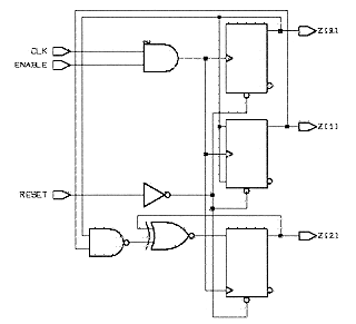
Figure 8.15 Design with AND Gate on Clock and Enable Signals