
Synchronous Mode Debugging
You must first download your design before you can debug it. The synchronous mode requires an interface, the XChecker cable, which enables you to conduct a controlled readback of your design. In this debug mode, you control the clock through the XChecker cable.
The snapshot and clock features, which are available when performing synchronous mode debugging, enable you to define specific clock patterns to gather the device states you want. For example, if you are debugging a counter, you may want to check that the combinational values generate the state value of 10. Set the Number of Clocks Before First Snapshot to 10 and the number of snapshots to 1 to capture state 10 of the device.
In addition, you can use the following options.
- Start Clock
This option establishes a free-running clock on the CLKO pin and advances the states of the device forward.
- Stop Clock
This option stops the clock being applied on the CLKO pin.
- Reset FPGA
This option uses an active-Low pulse to set the device to its initial state.
- Apply CLKO Clock(s)
This option moves the device forward the number of states set by the Number of CLKO Clocks to Apply option.
Pin Assignments
Before enabling the Synchronous Mode, choose whether you want to use an internal XChecker clock or an external clock connected to the XChecker CLKI pin.
- To use the internal XChecker clock, connect the CLKO pin to the FPGA system clock input pin in place of an oscillator. Leave the CLKI pin unconnected.
- To use an external CLKI clock, connect the system clock to the XChecker CLKI pin and connect the XChecker CLKO pin to the FPGA system clock input pin.
Debugging in the Synchronous Mode
To debug in the synchronous mode, follow these steps.
- Select Debug
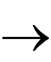 Synchronous Mode or click the following toolbar button.

The Debug  Settings commands and the Debug Control Panel options, shown in the “Debug Control Panel (Synchronous Mode)” figure, are enabled for synchronous debugging.
- Select Debug
 Settings
  CLKO Clock Source or click the Clocks button in the Debug Control Panel.
The CLKO Clock Settings dialog box appears as shown in the “CLKO Clock Settings Dialog Box” figure.
- Click the appropriate radio button for the clock you want to use: Use XChecker Clock or Use CLKI.
- If you select the XChecker Clock, set the clock frequency (0.921, 2.764, 5.529, or 11.059 MHz).
- If you select the CLKI clock, the FPGA uses the system clock connected to the XChecker CLKI pin. In this case, you cannot set the clock speed. The list box for the clock frequency is disabled.
- After setting the desired clock settings, click OK.
The CLKO Clock Settings dialog box closes and the status bar displays the clock settings.
- Select Debug
 Settings
  Trigger or click the Trigger button in the Debug Control Panel.
The Trigger command invokes the Synchronous Trigger Settings dialog box, shown in the “Synchronous Trigger Settings Dialog Box” figure, which enables you to select the type of trigger you want to initiate the readback.
- In the Trigger On list box, select External pin (active-High on the TRIG pin of the XChecker cable) or Enter Key to initiate a readback, or you can initiate a readback Immediately after the Read Snapshots command is executed.
- In the Number of Clock Cycles field, specify the number of clock cycles to apply before the first snapshot and between snapshots. Use these options to cycle the device before the first snapshot and between multiple snapshots.
- Use the Timeout After option to specify the cutoff time for a trigger to be detected. If the trigger is not received within the specified time, the readback is canceled.
- Select Pulse RESET at First Snapshot to reset the device each time you execute the Read Snapshots command.
- After setting the desired trigger settings, click OK.
The Synchronous Trigger Settings dialog box closes and the status bar displays the Trigger settings.
- Select Debug
 Settings
  Display Signals or click the Display button in the Debug Control Panel to choose the signals and groups that you want to display.
For details on how to select signals for display, see the “Creating and Modifying a Signal List” section in this chapter.
- Select Debug
 Settings
  Number of Snapshots to Read or type a number in the Number of Snapshots field in the Debug Control Panel.
The Snapshots Count dialog box appears, as shown in the “Snapshots Count Dialog Box” figure, allowing you to enter the number of snapshots to read.
- After setting the desired number of snapshots, click OK.
The Snapshots Count dialog box closes and the status bar displays the number of snapshots.
- Select Debug
 Read Snapshots or click Read in the Debug Control Panel to read the states of the signals that you selected for debugging.
The device being read back returns its configuration data and the state of every probe point when a readback is triggered.
The software then extracts the signals you selected and displays the signal values in a waveform, as shown in the “Waveform Window” figure.
NOTEThe readback data stream is linked to the active waveform window only. After the connection is closed, the waveform window is not updated with new information.
|
Cycling the Device
One aspect of controlling the clock through the XChecker cable consists of applying a specific number of clocks to the device. When you apply clocks to your device, you advance the state of your device.
Use the Apply CLKO Clock(s) command to apply the number of clocks specified with the Number of CLKO Clocks to Apply command.
- Select Debug
 Settings
  Number of CLKO Clocks to Apply and enter the number of clocks to apply or type a number in the Number of Clocks field in the Debug Control Panel.
- Select Debug
 Apply CLKO Clock(s) to cycle the device the number of clocks specified in the Number of Clocks to Apply field. Alternatively, you can click Apply in the Debug Control Panel.
NOTEWhen the number of clocks to apply is set to 1, the Apply Clocks command can be used to single step the device during synchronous debugging.
|
Resetting the FPGA
If you have not set the Pulse RESET at First Snapshot option in the Trigger Settings dialog box, choose Debug  Reset FPGA to issue an active-Low reset before issuing the Read Snapshots command.
Viewing Additional Signals
To view new signals on your waveform, you must add these signals to the display list and read the device states again.
- Use the Debug
 Settings
  Display Signals command or click Display in the Debug Control Panel to add new signals to the display list.
- In the Display Signals dialog box, add the new signals to the display.
- Click OK.
- Select Debug
 Read Snapshots to read the states of the new signals.
Viewing the Waveform in Text Mode
Select View  Text Data to display the snapshots in textual form.


![]() Reset FPGA to issue an active-Low reset before issuing the Read Snapshots command.
Reset FPGA to issue an active-Low reset before issuing the Read Snapshots command.![]() Text Data to display the snapshots in textual form.
Text Data to display the snapshots in textual form.