| XC3000 | XC4000E | XC4000X | XC5200 | XC9000 | Spartan | SpartanXL | Virtex |
|---|---|---|---|---|---|---|---|
| N/A | N/A | Primitive | Macro | N/A | N/A | Primitive | Primitive |
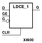
LDCE_1 is a transparent data latch with asynchronous clear, gate enable, and inverted gate. When the asynchronous clear input (CLR) is High, it overrides the other inputs and resets the data (Q) output Low. Q reflects the data (D) input while the gate (G) input and CLR are Low and gate enable (GE) is High. If GE is Low, the data on D cannot be latched. The data on the D input during the Low-to-High gate transition is stored in the latch. The data on the Q output remains unchanged as long as G remains High or GE remains Low.
The latch is asynchronously cleared with Low output when power is applied. FPGAs simulate power-on when global reset (GR) or global set/reset (GSR) is active. GR (XC5200) and GSR (XC4000X, SpartanXL, Virtex) default to active-High but can be inverted by adding an inverter in front of the GR/GSR input of the STARTUP or the STARTUP_VIRTEX symbol.
| Inputs | Outputs | |||
|---|---|---|---|---|
| CLR | GE | G | D | Q |
| 1 | X | X | X | 0 |
| 0 | 0 | X | X | No Chg |
| 0 | 1 | 0 | 0 | 0 |
| 0 | 1 | 0 | 1 | 1 |
| 0 | 1 | 1 | X | No Chg |
| 0 | 1 | D | d | |
| d = state of input one setup time prior to Low-to-High gate transition | ||||
Figure 7.12 LDCE_1 Implementation XC5200 |