The output of PAR is a placed and routed NCD file (the output design file). In addition to the output design file, a PAR run generates a report file with a .par extension, a delay file with a .dly extension, and a pinout file with a .pad extension. The PAR file contains execution information about the place and route job as well as all constraint messages. The DLY file contains delay information about the routed nets in the design. The PAD file lists IOBs (Input/Output Blocks) on the chip and the primary pins associated with the IOBs.
If the options that you specify when running PAR are options that produce a single output design file, your output is the output design file, a PAR file, a DLY file, and a PAD file. The PAR file, the DLY file, and the PAD file all have the same root name as the output design file.
If you run multiple iterations of placement and routing, you produce an output design file, a PAR file, a DLY file, and a PAD file for each iteration. Consequently, when you run multiple iterations you have to specify a directory in which to place these files.
As the command is performed, PAR records a summary of all placement and routing iterations in one PAR file at the same level as the directory you specified, then places the output files (in NCD format) in the specified directory. Also, a PAR file, a DLY file, and a PAD file are created for each NCD file, describing in detail each individual iteration.
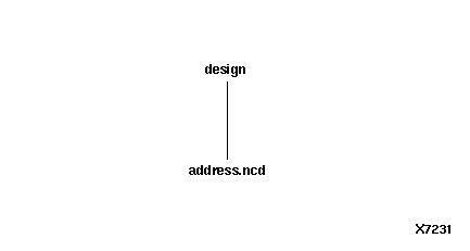
For example, suppose you have a directory named design with a design file called address.ncd, as shown in the following figure.
Suppose you run three iterations of place and route, using a different cost table entry each time (cost tables are explained in the “Placement” section) and specify that the resulting output be put into a directory called output.dir. The actual command would be
par -n 3 -l 1 address.ncd output.dir
-n 3 is the number of iterations you want to run, -l 1 sets the placement effort level, address.ncd is your input design file, and output.dir is the name of the directory in which you want to place the results of the PAR run.
The files resulting from the command are shown in the following figure.
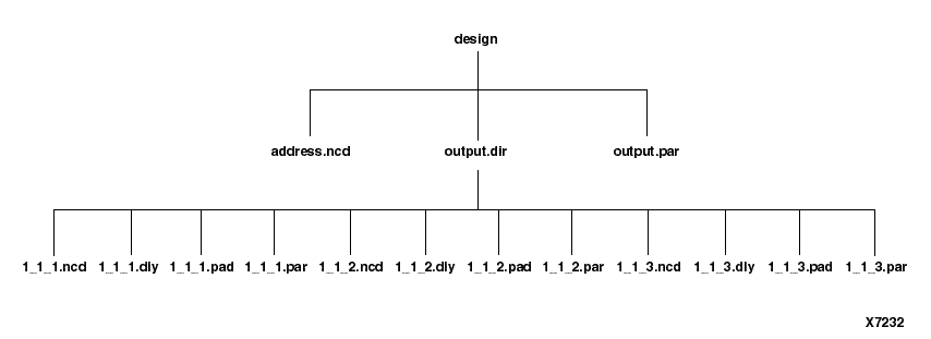
The naming convention for the files, which may contain placement and routing information in varying degrees of completion, is placer_level_router_level_table.file_extension.
In the sample above, the effort level and cost table entries start at 1 (the default value). The PAR, DLY, and PAD files are described in the following sections. When you run multiple iterations, you get a summary PAR report file like the one shown below.
The PAR Report is formatted for viewing in a monospace (non-proportional) font. If the text editor you use for viewing the report uses a proportional font, the columns in the report do not line up correctly.
PAR: Xilinx Place And Route M1.5.13.Copyright (c) 1995-1998 Xilinx, Inc. All rights reserved.Tue Apr 28 10:57:28 1998par -ol 3 -n 5 -i 20 main_pcb.ncd routed main_pcb.pcfConstraints file: main_pcb.pcfLevel/ Design Timing Number Run NCD
Cost [ncd] Score Score Unrouted Time Status
---------- ------ -------- -------- ----- ------------
3_3_3 * 737 0 0 04:55 Complete
3_3_5 * 748 0 0 05:13 Complete
3_3_4 * 756 0 0 05:12 Complete
3_3_1 * 773 0 0 06:00 Complete
3_3_2 * 816 0 0 05:22 Complete * : Design saved.PAR done.At the top of the summary PAR file is information regarding the software level, copyright information, and the date and time of the run. Directly below that is the command line used to run PAR, followed by the name of any physical constraints file used.
The body of the report consists of the following columns.
Level/Cost [ncd] - indicates the effort level (1-5) at which PAR is run. In the sample above, 3_3_4 indicates placer level 3, router level 3, and the fourth cost table used.
Design Score - see “The Place and Route (PAR) Report File” section.
Timing Score - see “The Place and Route (PAR) Report File” section.
Number Unrouted - indicates the number of unrouted nets in the design.
Run Time - the time required to complete the job in minutes and seconds.
NCD Status - describes the state of the output NCD file generated by the PAR run. Possible values for this column are
The place and route (PAR) report file contains execution information about the PAR command run. The file shows the steps taken as the program converges on a placement and routing solution. A sample PAR file is shown following.
The PAR Report is formatted for viewing in a monospace (non-proportional) font. If the text editor you use for viewing the report uses a proportional font, the columns in the report do not line up correctly.
PAR: Xilinx Place And Route M1.5.15.

   Copyright (c) 1995-1998 Xilinx, Inc.  All rights reserved.
Tue Apr 28 12:05:37 1998Constraints file: timing.pcfLoading device database for application par from file "x403-001.ncd".
"x403-001" is an NCD, version 2.27,device xc4028ex,package hq208, speed -3
Loading device for application par from file '4028ex.nph' in environment
/build/bcxfndry/rtf/x1_5.13.Device speed data version: x1_0.26 1.8 Device utilization summary: Number of External IOBs 60 out of 160 37%
Flops: 32
Latches: 0
Number of Global Buffer IOBs 4 out of 8 50%
Flops: 0
Latches: 0
Number of CLBs 94 out of 1024 9%
Total Latches: 0 out of 2048 0%
Total CLB Flops: 105 out of 2048 5%
4 input LUTs: 136 out of 2048 6%
3 input LUTs: 42 out of 1024 4% Number of BUFGLSs 4 out of 8 50%
Number of TBUFs 54 out of 2176 2%Overall effort level (-ol): 2 (default)
Placer effort level (-pl): 2 (default)
Placer cost table entry (-t): 1
Router effort level (-rl): 2 (default)
Timing method (-kpaths|-dfs): -kpaths (default)Starting initial Timing Analysis. REAL time: 47 secs
Finished initial Timing Analysis. REAL time: 1 mins 21 secs Starting initial Placement phase. REAL time: 1 mins 21 secs
Finished initial Placement phase. REAL time: 1 mins 36 secs Starting Constructive Placer. REAL time: 1 mins 43 secs
Placer score = 575479
Placer score = 362356
Placer score = 279001
.
.
.
Placer score = 57390
Placer score = 56110
Finished Constructive Placer. REAL time: 5 mins 15 secs
Writing design to file "routed.ncd".
Starting Optimizing Placer. REAL time: 5 mins 16 secs
Optimizing . . . .
Swapped 83 comps.
Xilinx Placer [1] 49960 REAL time: 6 mins 9 secs
Finished Optimizing Placer. REAL time: 6 mins 9 secs
Writing design to file "routed.ncd".
Total REAL time to Placer completion: 6 mins 11 secs
Total CPU time to Placer completion: 3 mins 1 secs
0 connection(s) routed; 836 unrouted active, 2 unrouted PWR/GND.
Starting router resource preassignment
Completed router resource preassignment. REAL time: 6 mins 19 secs
Starting iterative routing.
Routing active signals
End of iteration 1
836 successful; 0 unrouted active,
2 unrouted PWR/GND; (0) REAL time: 7 mins 14 secs
End of iteration 2
836 successful; 0 unrouted active,
2 unrouted PWR/GND; (0) REAL time: 7 mins 20 secs
Constraints are met.
Routing PWR/GND nets.
Power and ground nets completely routed.
Writing design to file "routed.ncd".
Starting cleanup
Improving routing.
End of cleanup iteration 1
838 successful; 0 unrouted; (0) REAL time: 10 mins 46 secs
Writing design to file "routed.ncd".
Total REAL time: 10 mins 47 secs
Total CPU time: 5 mins 21 secs
End of route. 838 routed (100.00%); 0 unrouted.
No errors found.
Completely routed.
Total REAL time to Router completion: 10 mins 51 secs
Total CPU time to Router completion: 5 mins 23 secs
Generating PAR statistics.
The Delay Summary Report
The Score for this design is: 673
The Number of signals not completely routed for this design is: 0
The Average Connection Delay for this design is: 3.890 ns
The Average Connection Delay on critical nets is: 0.000 ns
The Average Clock Skew for this design is: 1.173 ns
The Maximum Pin Delay is: 22.769 ns
The Average Connection Delay on the 10 Worst Nets is: 14.210 ns
Listing Pin Delays by value: (ns)
d <= 10 < d <= 20 < d <= 30 < d <= 40 < d <= 50 d > 50
--------- --------- --------- --------- --------- ---------
750 39 4 0 0 0
Timing Score: 0
-------------------------------------------------------------------------
Constraint | Requested | Actual | Logic
| | | Levels
-------------------------------------------------------------------------
NET "CTLR/2SCLK" PERIOD = 43.000000 nS | 43.000ns | 32.913ns | 2
-------------------------------------------------------------------------
NET "CTLR/SCLK" PERIOD = 45.000000 nS | 45.000ns | 30.140ns | 2
-------------------------------------------------------------------------
All constraints were met.
Writing design to file "routed.ncd".
All signals are completely routed.
Total REAL time to PAR completion: 11 mins 1 secs
Total CPU time to PAR completion: 5 mins 29 secs
PAR done.
Sometimes the design is completely routed, but the router continues to route in the attempt to meet timing constraints.
Note that in the sample PAR file above, in the “starting iterative routing” section, after the end of iteration 1, there is a figure in parentheses (0). This represents the timing score for the design (not to be confused with the PAR score) at the end of the particular iteration. This figure appears in the PAR file only when timing constraints have been specified in a PCF file. When the timing score is 0 (as it is in this example after iteration 1), this means that all timing constraints have been met. This score (0) also appears at the end of the delay report section of the PAR file.
The timing score at the end of the “starting iterative routing” section may not agree with the timing score in the Delay Summary Report. This can occur if a MAXSKEW constraint is scored and not met.
Had the design been completely routed but failed to meet all timing constraints, the score would have been a figure other than 0. A non-zero number would appear at the end of the delay report section. This tells you immediately whether your timing constraints have been met. It is possible that the timing score shown in parentheses at the top of the file may be different from the one shown in the delay summary section of the file. The score shown in the delay summary section is always the correct one.
The last section of the PAR file contains a summary of the delay information for the routed design. The DLY (delay) file produced by the PAR run contains more detailed timing information. The DLY file is discussed in the following section.
If you specify a command option that produces multiple output design files, there is a PAR file indicating all of the place and route iterations performed, and individual PAR files describing placement and routing for each design file produced.
NOTE
In PAR reporting, a tilde (~) preceding a delay value indicates that the delay value is approximate. Values with the tilde cannot be calculated exactly because of excessive delays, resistance, or capacitance on the net. You can use the PENALIZE TILDE constraint to penalize these delays by a specified percentage (see the “TRACE” chapter and the “Attributes, Constraints, and Carry Logic” chapter of the Libraries Guide for a description of the PENALIZE TILDE constraint).
Some notes about the entries in the PAR file.
- The Placer score is a rating of the relative “cost” of a placement. A lower score indicates a better (that is, less “costly”) placement.
- In the Delay Summary Report section of the PAR report file where average delays are listed (beginning with THE AVERAGE CONNECTION DELAY for this design), there are two columns of figures. The first column gives the actual averages for the design. The figures in the second column, which are enclosed by parentheses, indicate the averages after the imposition of a tilde penalty.
- The Score For This Design is a rating of the routed design. The score is discussed in the “Scoring the Routed Design” section.
- Timing score is always 0 (zero) if all timing constraints have been met. If not, the figure is other than 0.
For the Virtex devices, if more than one SelectIO standard is used, an additional section on Select IO utilization and usage summary is added to the PAR file. This section shows details for the different IO banks. It shows the IO standard, the output reference voltage (VCCO)] for the bank, the input reference voltage (VREF) for the bank, the PAD and Pin names. In addition, the section gives a summary for each bank with the number of pads being used, the voltages of the VREFs, and the VCCOs. A sample Select IO utilization and Usage Summary of the PAR file follows.
Select IO Utilization and Usage Summary
_______________________________________
NR - means Not Required.
Each Group of a specific Standard is listed.
IO standard (LVTTL Vref=NR Vcco=3.30) occupies 45 pads.
IO standard (CTT Vref=1.50 Vcco=3.30) occupies 8 pads.
IO standard (SSTL3_I Vref=0.90 Vcco=3.30) occupies 12 pads.
Bank Summary
____________
NR - means Not Required
Bank 0 has 20 pads and is 80% utilized.
Vref should be set to NR volts.
Vcco should be set to 3.30 volts.
Name IO Select Std Vref Vcco Pad Pin
---- -- ---------- ------ ------ ------ ------
bidir<7> IO LVTTL NR 3.30 PAD2 P238
bidir<6> IO LVTTL NR 3.30 PAD3 P237
bidir<3> IO LVTTL NR 3.30 PAD8 P231
bidir<1> IO LVTTL NR 3.30 PAD10 P230
b<10> I LVTTL NR PAD11 P229
.
.
.
b<7> I LVTTL NR PAD17 P221
a<10> I LVTTL NR PAD18 P220
Bank 1 has 22 pads and is 13% utilized.
Vref should be set to NR volts.
Name IO Select Std Vref Vcco Pad Pin
---- -- ---------- ------ ------ ------ ------
.
.
.
Bank 7 has 21 pads and is 38% utilized.
Vref should be set to 0.90 volts.
Vref sites in this bank cannot be used for user IOBs.
Vcco should be set to 3.30 volts.
Name IO Select Std Vref Vcco Pad Pin
---- -- ---------- ------ ------ ------ ------
bidir<11> IO SSTL3_I 0.90 3.30 PAD169 P28
bidir<8> IO SSTL3_I 0.90 3.30 PAD170 P27
bidir<9> IO SSTL3_I 0.90 3.30 PAD172 P25
bidir<10> IO SSTL3_I 0.90 3.30 PAD173 P24
c<9> O CTT 3.30 PAD181 P13
c<10> O CTT 3.30 PAD187 P7
c<7> O LVTTL 3.30 PAD190 P4
c<8> O CTT 3.30 PAD191 P3
Total REAL time to Placer completion: 40 secs
Total CPU time to Placer completion: 31 secs
The Delay (DLY) File
The delay file is output by each PAR run and is placed in the directory with the NCD output of the design file and the PAR file. The delay file contains delay information for each net in the design and includes
- A listing of the 20 nets with the longest delays., In a DLY file, maximum delays are preceded by a tilde, indicating that the delay shown is only approximate. Following each tilde delay is a figure in parentheses. This figure represents the approximate delay with a certain percentage automatically added to it (a “worst case” situation) when specified by the user in the physical constraints (PCF) file. When the Xilinx Development System's timing analysis software looks at the delays, it uses the value in parentheses rather than the approximate value represented by the tilde. For more information on the PENALIZE TILDE constraint, see the “TRACE” chapter in this manual and the “Attributes, Constraints, and Carry Logic” chapter of the Libraries Guide.
- A delay analysis for each net, including the net name, followed by the driver pin and the load pin(s).
The following is a portion of a delay file. If this were a complete file, it would show the load delays for all nets in the design.
NOTE
The Delay Report is formatted for viewing in a monospace (non-proportional) font. If the text editor you use for viewing the report uses a proportional font, the columns in the report do not line up correctly.
File: routed.dly
The 20 Worst Net Delays are:
-------------------------------
| Max Delay (ns) | Netname |
-------------------------------
22.769 CTLR/VID/MUX/RHORZ
19.962 CTLR/VID/MUX/RVERT
18.060 CTLR/VID/S3
15.488 CTLR/VID/VA6
15.009 CTLR/VID/MUX/AVERT
13.171 CTLR/VID/MUX/AHORZ
12.829 CTLR/VID/VA1
12.829 CTLR/VID/VA3
12.641 CTLR/VID/VA7
12.629 CTLR/VID/VA8
11.315 CTLR/VID/VA4
11.315 CTLR/VID/VA2
10.881 CTLR/PA9
10.486 CTLR/VID/VA0
10.197 CTLR/VID/VA5
9.541 CTLR/PA11
9.306 CTLR/PA13
9.180 CTLR/VISC/VCS_ACK
8.981 CTLR/ODM/EF7
8.941 CTLR/SCLK
---------------------------------
---------------------------------------------------- Net Delays
-----------------------------------------------------
2SCLK_I
2SCLK_I.CLKIN
0.100 CTLR/$1I293.I
ALE_I
ALE_I.CLKIN
0.100 CTLR/VISC/$1I354.I
CTLR/2SCLK
CTLR/$1I293.O
5.424 CTLR/ODM/FIFOCTRL/READ.F2
4.920 CTLR/ODM/FIFOCTRL/NS_FBYT_CE.K
4.902 CTLR/ODM/SE_FGEN/SEA2.K
4.913 CTLR/PA19.K
4.911 CTLR/PA18.K
.
.
.
The PAD File
The PAD file contains a listing of all IOBs used in the design and their associated pads. The file specifies connections to device pins (with a P prefix).
The PAD file is divided into three sections.
- The first section lists the component name in the first column. The second column of this section lists the designations of the device pins.
- The second section lists the pin number in the first column, the component name in the second column, and any constraints assigned to the component in the third column.
- The third section lists the pinouts in the form of constraints. These constraints can be cut and pasted into a PCF file as constraints for later PAR runs.
A sample PAD file is shown following.
NOTE
The PAD Report is formatted for viewing in a monospace (non-proportional) font. If the text editor you use for viewing the report uses a proportional font, the columns in the report do not line up correctly.
PAR: Xilinx Place And Route M1.5
Copyright (c) 1995-1998 Xilinx, Inc. All rights reserved.
Thu Apr 16 15:21:43 1998
Xilinx PAD Specification File
*****************************
Input file: x403-001.ncd
Output file: routed.ncd
Part type: xc4028ex
Speed grade: -3
Package: hq208
Tue Apr 28 12:16:35 1998
Pinout by Pin Name:
+------------------------------------------------+-----------+----------+
| Pin Name | Direction | Pin Number |
+------------------------------------------------+-----------+----------+
| 2SCLK_I | INPUT | P47 |
| A2I | INPUT | P31 |
| A3I | INPUT | P29 |
. .
. .
. .
| VIDCS_I- | INPUT | P174 |
| VOC_O | OUTPUT | P195 |
| WR_I- | INPUT | P149 |
+------------------------------------------------+-----------+----------+
| Dedicated or Special Pin Name | Pin Number |
+------------------------------------------------------------+----------+
| /PROGRAM | P108 |
| CCLK | P153 |
| DONE | P103 |
| GND | P101 |
. .
. .
. .
| VCC | P55 |
| VCC | P26 |
| VCC | P183 |
+------------------------------------------------------------+----------+
Pinout by Pin Number:
+--------------+-----------------------------------+-----------+--------+
| Pin Number | Pin Name | Direction | Constraint |
+--------------+-----------------------------------+-----------+--------+
| P1 | N.C. | | |
| P2 | GND | | |
| P3 | N.C. | | |
| P4 | SCLK_I | INPUT | |
. .
. .
. .
| P204 | SYSCLK_I | INPUT | |
| P205 | VCC | | |
| P206 | N.C. | | |
| P207 | N.C. | | |
| P208 | N.C. | | |
+--------------+-----------------------------------+-----------+--------+
#
# Pinout constraints listing
# These constraints are in PCF grammar format
# and may be cut and pasted into the PCF file
# after the "SCHEMATIC END ;" statement to
# preserve
COMP "2SCLK_I" LOCATE = SITE "P47" ;
COMP "A2I" LOCATE = SITE "P31" ;
COMP "A3I" LOCATE = SITE "P29" ;
.
.
.
COMP "VERT_O-" LOCATE = SITE "P178" ;
COMP "VIDCS_I-" LOCATE = SITE "P174" ;
COMP "VOC_O" LOCATE = SITE "P195" ;
COMP "WR_I-" LOCATE = SITE "P149" ;
For the Virtex devices, when SelectIOs are used, the PAD file also contains details of the pads that must be used for the input reference voltage (VREF), and those that must be used for the output reference voltage (VCCO). For the VREF pads, their location and the value of the input reference voltage is shown. A sample Virtex PAD file follows.
PAR: Xilinx Place And Route M1.5.13.
Copyright (c) 1995-1998 Xilinx, Inc. All rights reserved.
Wed May 6 10:15:49 1998
Xilinx PAD Specification File
*****************************
Input file: virtex_test.ncd
Output file: virtex_test.out.ncd
Part type: xcv50
Speed grade: -5
Package: pq240
Wed May 6 10:15:49 1998
Pinout by Pin Name:
+------------------------------------------------+-----------+----------+
| Pin Name | Direction | Pin Number |
+------------------------------------------------+-----------+----------+
| a<0> | INPUT | P97 |
| a<1> | INPUT | P99 |
| a<2> | INPUT | P103 |
| a<3> | INPUT | P113 |
.
.
.
+------------------------------------------------+-----------+----------+
| Dedicated or Special Pin Name | Pin Number |
+------------------------------------------------------------+----------+
| CCLK | P179 |
| DONE | P120 |
| GND | P14 |
.
.
.
| VCCO | P197 |
| VCCO | P105 |
| VREF (0.90V) | P9 |
| VREF (0.90V) | P70 |
| VREF (0.90V) | P84 |
| VREF (1.50V) | P36 |
| VREF (1.50V) | P50 |
+------------------------------------------------------------+----------+
Pinout by Pin Number:
+--------------+-----------------------------------+-----------+--------+
| Pin Number | Pin Name | Direction | Constraint |
+--------------+-----------------------------------+-----------+--------+
| P1 | GND | | |
| P2 | TMS | | |
.
.
.
| P9 | VREF (0.90V) | | |
| P36 | VREF (1.50V) | | |
| P61 | VCCO | | |
+--------------+-----------------------------------+-----------+--------+
#
# Pinout constraints listing
# These constraints are in PCF grammar format
# and may be cut and pasted into the PCF file
# after the "SCHEMATIC END ;" statement to
# preserve this pinout for future design iterations.
#
.
.
.
