


![]()
1. Double-click the targeted device icon ![]() .
The Device Properties dialog box appears. This dialog allows you to
select from a CPLD family.
.
The Device Properties dialog box appears. This dialog allows you to
select from a CPLD family.
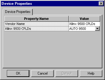
2. Click the Vendor Name Value and 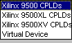 the Xilinx CPLD families appear. Select a family (Xilinx 9500 CPLDs
are selected above) from the list, then click in the Value box on
the second row to select specific devices and packages. The
following drop-down will appear.
the Xilinx CPLD families appear. Select a family (Xilinx 9500 CPLDs
are selected above) from the list, then click in the Value box on
the second row to select specific devices and packages. The
following drop-down will appear. 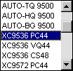 Select a target device or leave it on AUTO and the fitter will pick
the smallest device and package that will fit your design, and give
you the fastest speed grade available for that device/package. You
can also select AUTO for specific package types (such as AUTO-VQ
9500) and the fitter will automatically select for your design the
smallest device and smallest pin count within the selected package type.
Select a target device or leave it on AUTO and the fitter will pick
the smallest device and package that will fit your design, and give
you the fastest speed grade available for that device/package. You
can also select AUTO for specific package types (such as AUTO-VQ
9500) and the fitter will automatically select for your design the
smallest device and smallest pin count within the selected package type.
You may also select specific device/package combinations (such as XC9536-VQ44). If you want to assign device pins, select a specific device/package combination.
3. Before running the fitter, you
may wish to set some of the fitter options. With the targeted device icon ![]() and the Fit Design process highlighted, select Process
- Properties. The Process
Properties dialog box will appear.
and the Fit Design process highlighted, select Process
- Properties. The Process
Properties dialog box will appear.
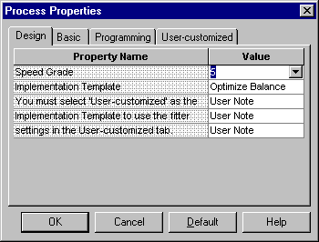
If you selected a specific device/package combination, you can also select a specific speed grade. With the Design tab selected, click on the Speed Grade Value and select a speed grade from the drop-down list. Then click OK. By default, the fastest speed grade for the targeted device is selected.
4. Select the Implementation Template you would like to use to control fitter optimization. The default template is Optimize Balance, which is a good starting point for a new design. Other options on the drop-down menu are Optimize Speed and Optimize Density, depending on your design needs.
If you want to manually control fitter optimization parameters, select User Customized on the Implementation Template drop-down menu.
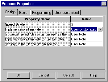
Then click the User-customized tab on the Process Properties dialog box to display the implementation options.
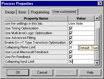
Adjust the optimization properties as needed. See the Implementations Options or design techniques section for more information on implementation options.
5. Next, fit the design. With the
targeted device icon ![]() and the Fit Design process highlighted, select Process
- Run. The fitter will run. After successfully completing, a
check will appear next to Fit Design, and the transcript will display
the success or failure of the fitter.
and the Fit Design process highlighted, select Process
- Run. The fitter will run. After successfully completing, a
check will appear next to Fit Design, and the transcript will display
the success or failure of the fitter.
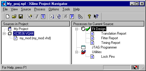
6. You can now examine any of the reports by double-clicking on the report name under the Fit Design process. The primary fitter results can be found in the Fitter Report and Timing Report.
7. Each time you implement your design, a guide file is created (design_name.gyd) which contains your pinout information. When you are ready to commit the pinout of your design, run the Lock Pins process under the Fit Design process. The pinout information stored in the .gyd file is appended to the end of the User Constraint File for your design (design_name.ucf). This pinout will then be applied to all subsequent design iterations run through the fitter.
When you run the Lock Pins process,
a report file is displayed which shows any pin assignment conflicts
which may have occurred.