

Specifying fMAX
You can specify the fMAX (clock frequency or period) for all registered paths
in your design using a Register-to-Register timespec. Register-to-Register
paths begin at flip-flop clock inputs, propagate through the flip-flop Q output and
any number of levels of combinatorial logic and end at the receiving flip-flop
D/T input, including the receiving flip-flop’s tSU. When these flip-flops are clocked by the same clock, the delay on this
path is equivalent to the cycle time of the clock.
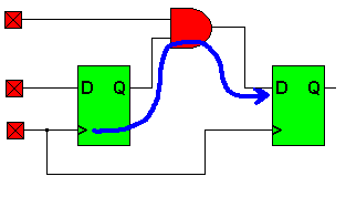
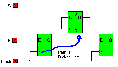
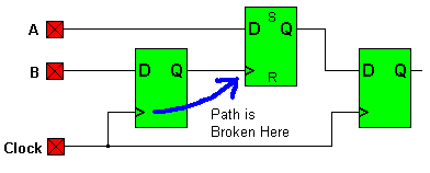
Registered paths do not propagate through clock, and asynchronous set and
reset inputs of registers as shown below. These paths are also broken at
bidirectional pins.
To specify fMAX, the maximum required operating frequency, compute the cycle
time and use the cycle time as the value in the timing constraint.
The format of the Register-to-Register timespec is:
TSnn=FROM:flip_flop_group:TO:flip_flop_group:delay_value
The following timing constraint specifies that fMAX for all registered paths
in the design is 67 Mhz:
TS01=FROM:FFS:TO:FFS:15
The next timing constraint specifies that fMAX between a specific pair of
registers is 66 Mhz:
TS02=FROM:FFS(REG1):TO:FFS(REG2):15
You can also use the Period timespec to define the maximum period of any clock
input, including the register-to-register paths between all flip-flops
controlled by the same clock:
TSnn=PERIOD:clock_group:period_value
For example, if the clock input CLOCK was contained in a timing group named
CLK_GRP, the following would specify a period of 15ns for all paths between all
flip-flops clocked by CLOCK:
TS01=PERIOD:CLK_GRP:15
To use the PERIOD form of timespec shown above, you could either attach the
attribute “TNM=CLK_GRP” to the CLOCK input pad or specify the group definition “CLK_GRP=PADS(CLOCK)” on a TIMEGRP symbol.
See Also
Entering Timespecs in a UCF File
Grouping Signals
Speeding Up fMAX with Local Feedback