

Memory Address Decoder
Design Specification
The following figure shows the block diagram for this design and a continuous
block of memory divided into four sections containing DRAM, I/O, ROM1 and ROM2.
The purpose of this decoder is to monitor the six high-order bits (A15-A10) of
a sixteen-bit address bus and select the correct section of memory based on
the value of these address bits.
The address ranges associated with each section of memory are shown as
follows. These address ranges can also be seen in the source file.
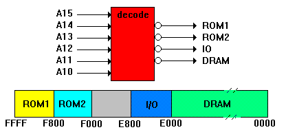
| Memory
Section | Address
Range (Hex) |
| DRAM
| 0000-DFFF
|
| I/O
| E000-E7FF
|
| ROM2
| F000-F7FF
|
| ROM1
| F800-FFFF
|
The following figure shows a simplified block diagram for the address decoder. The decoder is implemented with equations employing relational and logical operators as shown in the Memory Address Decoder Source File below.
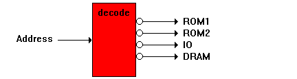
Significant simplification is achieved by grouping the address bits into a set named Address. The ten address bits that are not used for the address decode are given no-connect values in the set, indicating that the address in the overall design (that beyond the decoder) contains 16 bits, but that bits 0-9 do not affect the decode of that address and are not monitored. In contrast, defining the set as:
Address = [A15,A14,A13,A12,A11,A10]
ignores the existence of the lower-order bits. Specifying all 16 address lines as members of the address set allows full 16-bit comparisons of the address value against the ranges above.
Test Vectors
In this design, the test vectors are a listing of the values that must appear on the output lines for specific address lines for specific address values. The address values are specified in hexadecimal notation.
Memory Address Decoder Source File
module decode
title `memory decode`
A15,A14,A13,A12,A11,A10 pin;
ROM1,IO,ROM2,DRAM pin istype `com`;
H,L,X = 1, 0, .X. ;
Address = A15,A14,A13,A12, A11,A10,X,X, X,X,X,X, X,X,X,X;
equations
!DRAM = (Address <= ^hDFFF);
!IO = (Address >= ^hE000) & (Address <= ^hE7FF);
!ROM2 = (Address >= ^hF000) & (Address <= ^hF7FF);
!ROM1 = (Address >= ^hF800);
test_vectors
(Address -> [ROM1,ROM2,IO,DRAM])
^h0000 -> [ H, H, H, L ];
^h4000 -> [ H, H, H, L ];
^h8000 -> [ H, H, H, L ];
^hC000 -> [ H, H, H, L ];
^hE000 -> [ H, H, L, H ];
^hE800 -> [ H, H, H, H ];
^hF000 -> [ H, L, H, H ];
^hF800 -> [ L, H, H, H ];
end