Foundation Series 2.1i User GuideChapter 5: Design Methodologies - HDL Flow
All-HDL Designs
The following procedure describes the HDL flow for designs that are HDL only, that is, there are no schematics or instantiated LogiBLOX, netlist, or state machine macros.
Creating the Design
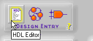
- Open the HDL Editor by clicking the HDL Editor icon in the Design Entry box on the Project Manager's Flow tab.
- When the HDL Editor window appears, you may select an existing HDL file or create a new one. The following steps describe creating a new HDL file with the Design Wizard.
- When the HDL Editor dialog box displays, select Use HDL Design Wizard. Click OK.
- Click Next in the Design Wizard window.
- From the Design Wizard - Language window, select VHDL or Verilog. Click Next.
Note: For top-level ABEL designs, you must use the Schematic Flow.
- In the Design Wizard - Name window, enter the name of your design file. Click Next.
- Define your ports in the Design Wizard-Ports window by clicking NEW, entering the port name, and selecting its direction. Click Finish. The Wizard creates the ports and gives you a template (in VHDL or Verilog) in which you can enter your design.
- Create the design in the HDL Editor. The Language Assistant is available to help with this step. It provides a number of language templates for basic language constructs and synthesis templates for synthesis-oriented implementation of basic functional blocks, such as multiplexers, counters, flip-flops, etc. Access the Language Assistant by selecting Tools
 Language Assistant.
- Add the design to the project by selecting Project Add to Project.
- Exit the HDL Editor.
For more information about HDL designs, see the“HDL Design Entry and Synthesis” chapter or, in the HDL Editor window, select Help Help Topics.
Analyzing Design File Syntax
Syntax is checked automatically when the design is added to the project. You can initiate a syntax check in the HDL Editor by selecting Synthesis Check Syntax. You can also analyze syntax by selecting Project Analyze All Sources from the Project Manager.
Use the HDL Error and HDL Warnings tabs in the messages area at the bottom of the Project Manager to view any syntax errors or messages output during analysis.
Performing HDL Behavioral Simulation (Optional)
If you installed an HDL simulation tool such as ACTIVE-VHDL or ModelSIM, you can perform a behavioral simulation of your HDL code. Please refer to the documentation provided with these tools for more information.
Synthesizing the Design
After the design files have been successfully analyzed, the next step is to translate the design into gates and optimize it for a target architecture. These steps are performed by running the Synthesis phase.
- Set the global synthesis options by selecting Synthesis Options from the Project Manager. In the Synthesis Options dialog, you can set the following defaults:
- Default clock frequency
- Export timing constraints to the place and route software
- Input XNF bus style
- FSM Encoding (One Hot or Binary)
- FSM Synthesis Style
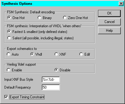
- Click OK to close the Synthesis Options dialog
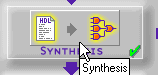
- Click the Synthesis icon on the Synthesis button on the Flow tab.
- The Synthesis/Implementation dialog box is displayed if this is the first version and revision of a project. (By default on subsequent runs, the same settings are used and the given version is overwritten. To create a new version, or to change settings, select Project Create Version.)
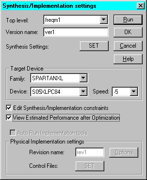
- Select the name of the top-level module. Processing will start from the file named here and proceed through all its underlying modules.
- Enter a version name.
- Select the target device.
- If you have Foundation Express, you have the following two options.
- Edit Synthesis/Implementation Constraints. Selecting this options pauses synthesis processing after the elaboration phase to allow you to specify constraints for the design using the Express Constraints Editor GUI. For more information refer to the “Express Constraints Editor” section.
- View Estimated Performance after Optimization. Select this option to view the estimated performance results after design optimization using the Express Time Tracker GUI. For more information refer to the “Express Time Tracker” section.
- Click Set to access the Settings dialog box containing Synthesis Setting for this version.
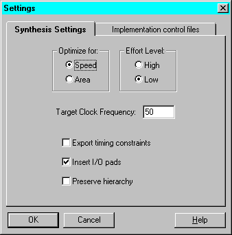
Modify the Synthesis Settings as desired.
- Modify the target clock frequency
- Select the optimization strategy as speed or area
- Select the effort level as high or low
- Select whether I/O pads should be inserted for the designated top-level module
Click OK to return to the Synthesis/Implementation Settings dialog box.
- Click OK to synthesize the designated top-level design and its underlying modules. (Or, click Run to synthesis and implement the design.)
The synthesis compiler automatically inserts top-level input and output pads required for implementation (unless instructed not to do so in the Synthesis Settings).
Express Constraints Editor
The Express Constraints Editor is available with the Foundation Express product only. It allows you to set performance constraints and attributes before optimization of FPGA designs.
- The Express Constraints Editor window automatically displays during Synthesis processing if you checked the Edit Synthesis/Implementation Constraints box on the Synthesis/Implementation dialog.
Alternatively, you can access the Express Constraints Editor via the Versions tab by right-clicking on the functional structure of a project version or functional structure in the Hierarchy Browser and then selecting Edit Synthesis Constraints.
The following figure shows an example of the Clocks tab of the Express Constraints Editor.
- Design-specific information is extracted from the design and displayed in device-specific spreadsheets. Click the tabs to access the various spreadsheets.
If you unchecked Insert I/O pads on the Synthesis/Implementation dialog, only the Modules and Xilinx Options tabs are shown. The Clocks, Ports, and Paths tabs apply only to top-level HDL designs.
- Right-click on an item in any of the spreadsheets to edit the value, access a dialog box to edit the value, or access a pulldown menu to select a value. Use the online help in the dialog boxes to understand and enter specific constraints and options.
The following figure shows an example of the dialog box accessed when you right click on an output delay value displayed on the Ports tab of the Express Constraints Editor.
- Optionally, you can import a constraints file (.exc) to use now (click Import Constraints) or you can export the entered constraints to a constraints file (.exc) for reuse (click Export Constraints).
- After you finish editing the constraints, click OK to close the Constraints window and continue the synthesis using the specified constraints.
Express Time Tracker
The Express Time Tracker is available with the Foundation Express product only. It allows you view estimated performance results after optimization of your design.
- The Optimized (Constraints) window, shown in the figures at the end of this section, automatically displays after Synthesis processing if you checked the View Estimated Performance after Optimization box in the Synthesis/Implementation dialog window.
Alternatively, you can access the Optimized (Constraints) window via the Versions tab by right-clicking on an optimized structure in the Hierarchy Browser and then selecting View Synthesis Results.
- Click the tabs to access the performance results in the various spreadsheets.
If you unchecked Insert I/O pads on the Synthesis/Implementation dialog, only the Models and Xilinx Options tabs are shown. The Clocks, Ports, and Paths tabs apply only to top-level HDL designs.
- After you finish viewing the results, click OK to close the Optimized (Constraints) window.
Performing Functional Simulation
Functional Simulation may be performed to verify that the logic you created is correct. Gate-level functional simulation is performed after the design is synthesized.
Note: There are several ways to apply stimulus and simulate a design. This section discusses one way: using the stimulator dialog. For more information on using the simulator, refer to its online help.
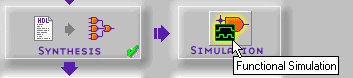
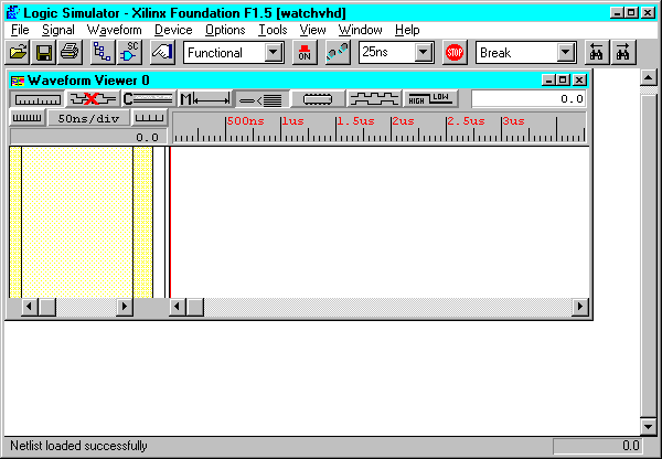
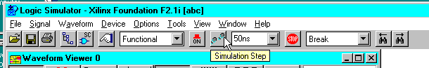
- Open the Logic Simulator by clicking the Functional Simulation icon in the Simulation box on the Project Manager's Flow tab.
- The design is automatically loaded into the simulator. The Waveform Viewer window displays inside of the Logic Simulator window.
- Add signals by selecting Signal Add Signals.
- From the Signals Selection portion of the Components Selection for Waveform Viewer window, select the signals that you want to see in the simulator.
- Use CTRL-click to select multiple signals. Make sure you add output signals as well as input signals.
- Click Add and then Close. The signals are added to the Waveform Viewer in the Logic Simulator screen.
- Select Signal Add Stimulators from the Logic Simulator menu. The Stimulator Selection window displays.
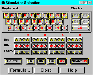
- In the Stimulator Selection window, create the waveform stimulus by attaching stimulus to the inputs. For more details on how to use the Stimulus Selection window, click Help.
- After the stimulus has been applied to all inputs, click the Simulator Step icon on the Logic Simulator toolbar to perform a simulation step. The length of the step can be changed in the Simulation Step Value box to the right of the Simulation Step box. (If the Simulator window is not open, select View Main Toolbar.)
- To save the stimulus for future viewing or reuse, select File Save Waveform. Enter a file name with a .tve extension in the File name box of the Save Waveform window. Click OK.
For more information about saving and loading test vectors, select Help Logic Simulator Help Contents from the Logic Simulator window. From the Help Index, select Working With Waveforms Saving and Loading Waveforms.
Implementing the Design
Design Implementation is the process of translating, mapping, placing, routing, and generating a Bit file for your design. Optionally, it can also generate post-implementation timing data.
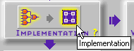
- Click the Implementation icon on the Implementation phase button on the Project Manager's Flow tab.
- The Synthesis/Implementation dialog box appears if the implementation is out-of-date.
A revision represents an implementation run on the selected-version. Modify the name in the Revision Name box, if desired. The synthesis settings are grayed out if synthesis has already been run.
- Click Set to access the Implementation control files dialog box. Identify any guide file, constraints file, or Floorplan file to use for this implementation.
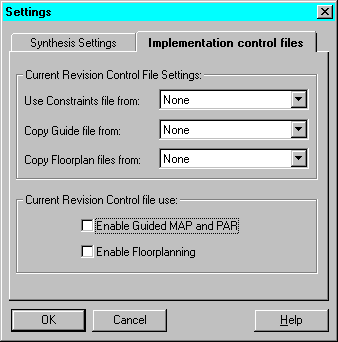
Click OK to return to the Synthesis/Implementation Settings dialog box.
- Click Options on the Synthesis/Implementation dialog box to set the Place and Route Effort level and edit implementation, simulation, or configuration options, if desired.
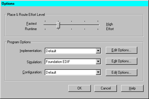
Click OK to return to the Settings/Implementation Settings dialog box.
- Click Run to implement the design. The Flow Engine displays the progress of the implementation.
The Project Manager displays a status message when Implementation is complete. View the Console tab on the Project Manager window for the results of all stages of the implementation. The Versions tab also indicates the status of the implemented revision.
- To view design reports, select the desired revision in the Versions tab of the Project Manager. Then select the Reports tab in the Project Manager Flow window.
Click on the Implementation Report Files icon to view the implementation reports. Click on the Implementation Log File icon to view the Flow Engine's processing log.
For more information on the Flow Engine, select Help Foundation Help Contents Flow Engine.
Editing Implementation Constraints
Design constraints affect how the logical design is implemented in the target device. Applying constraints helps you to adapt your design's performance to expected worst-case conditions. The user constraint file (.ucf) is an ASCII file that holds timing and location constraints. It is read (by NGDBuild) during the translate process in the Flow Engine and is combined with an EDIF or XNF netlist into an NGD file.
Each revision contains an associated UCF file. The UCF file may be a default (empty) UCF or one that you customize yourself. You can directly enter constraints in the UCF file through a text editor or you can use the Xilinx Constraints Editor.
- The Constraints Editor is a Graphical User Interface (GUI) that you can run after the Translate program to create new constraints in a UCF file. To access the Constraints Editor, select Tools Implementation Constraints Editor from the Project Manager.
The following figure shows an example of the Global tab of the Implementation Constraints Editor.
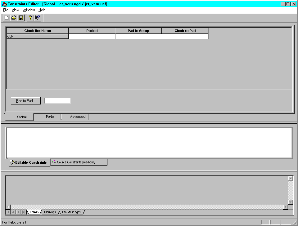
- Design-specific information is extracted from the design and displayed in device-specific spreadsheets. Click the tabs to access the various spreadsheets.
- Right-click on an item in any of the spreadsheets to access a dialog box to edit the value. Use the online help in the dialog boxes to understand and enter specific constraints and options. Or, refer to the online software document, Constraints Editor Guide for detailed information.
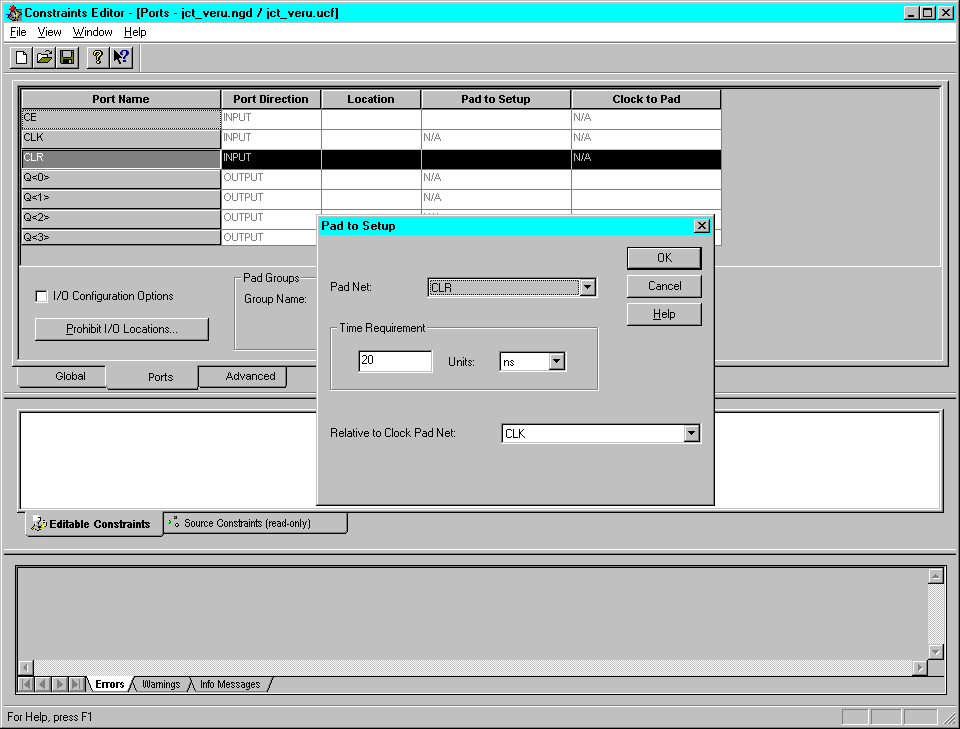
The following figure shows an example of the Pad to Setup dialog box accessed when you right click anywhere on a Port row on the Ports tab of the Implementation Constraints Editor and then select Pad to Setup.
- After you finish editing the constraints, click Save to close the Constraints Editor window
- You must rerun the Translate step in the Flow Engine to have your new constraints applied to the design.
- Click the Implementation icon on the Project Manager's Flow tab to rerun Translate and the rest of the flow.
Verifying the Design
After the design has been implemented, the Timing Analyzer or the Timing Simulator can be used to verify the design. The Timing Analyzer performs a static timing analysis of the design. The Timing Simulator uses worst-case delays and user input stimulus to simulate the design.
Performing a Static Timing Analysis
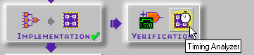
- Click the Timing Analyzer icon in the Verification box on the Project Manager's Flow tab to perform a static timing analysis.
- For FPGAs, you can perform a post-MAP, post-place, or post-route timing analysis to obtain timing information at various stages of the design implementation. You can perform a post-implementation timing analysis on CPLDs after a design has been fitted.
For details on how to use the Timing Analyzer, select Help Foundation Help Contents Timing Analyzer.
Performing a Timing Simulation
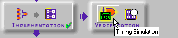
- Open the Timing Simulator by clicking the Timing Simulation icon in the Verification box on the Project Managers's Flow tab. The implementation timing netlist with worst-case delays will be loaded into the simulator.
The Waveform Viewer window displays inside the Logic Simulator window.
- Refer to the “Performing Functional Simulation” section earlier in this chapter for instructions on simulating the design. (The operation of the simulator is the same for functional and timing simulation.)
- If you have already saved test vectors (for instance, in the functional simulation), you may load these vectors into the timing simulator by selecting File Load Waveform.
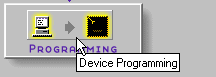
Programming the Device
- Click the Device Programming icon in the Programming box on the Project Manager's Flow tab.
- From the Select Program box, choose the Hardware Debugger, the PROM File Formatter, or the JTAG Programmer. For CPLD designs, use the JTAG Programmer. For instructions, select Help Foundation Help Contents Advanced Tools JTAG Programmer. For FPGA designs, use the JTAG Programmer, Hardware Debugger, or PROM File Formatter. For instructions, select Help Foundation Help Contents Advanced Tools and then select the desired tool.