|
|
|
|
This appendix presents examples that demonstrate basic concepts of Foundation Express.
The following figure is a diagram of a simple Moore finite state machine. It has one input (X), four internal states (S0 to S3), and one output (Z).
Moore Machine Specification
The VHDL code implementing this finite state machine is shown in the following example, which includes a schematic of the synthesized circuit.
The machine description includes two processes. One process defines the synchronous elements of the design (state registers); the other process defines the combinatorial part of the design (state assignment case statement). For more details on using the two processes, see the “Combinatorial Versus Sequential Processes” section of the “Sequential Statements” chapter.
entity MOORE is               -- Moore machine

  port(X, CLOCK: in BIT;

       Z: out BIT);

end MOORE;
architecture BEHAVIOR of MOORE is

  type STATE_TYPE is (S0, S1, S2, S3);

  signal CURRENT_STATE, NEXT_STATE: STATE_TYPE;

begin
  -- Process to hold combinatorial logic

  COMBIN: process(CURRENT_STATE, X)

  begin

    case CURRENT_STATE is

      when S0 =>

        Z <= '0';

        if X = '0' then

          NEXT_STATE <= S0;

        else

          NEXT_STATE <= S2;

        end if;

      when S1 =>

        Z <= '1';

        if X = '0' then

          NEXT_STATE <= S0;

        else

          NEXT_STATE <= S2;

        end if;

      when S2 =>

        Z <= '1';

        if X = '0' then

          NEXT_STATE <= S2;

        else

          NEXT_STATE <= S3;

        end if;

      when S3 =>

        Z <= '0';

        if X = '0' then

          NEXT_STATE <= S3;

        else

          NEXT_STATE <= S1;

        end if;

    end case;

  end process COMBIN;
  -- Process to hold synchronous elements (flip-flops)

  SYNCH: process

  begin

    wait until CLOCK'event and CLOCK = '1';

    CURRENT_STATE <= NEXT_STATE;

  end process SYNCH;

end BEHAVIOR;
Moore Machine Schema tic
The following figure is a diagram of a simple Mealy finite state machine. The VHDL code for implementing this finite state machine is shown in the example following the diagram. The machine description includes two processes, as in the previous Moore machine example.
Mealy Machine Specifi cation
entity MEALY is            -- Mealy machine

  port(X, CLOCK: in BIT;

       Z: out BIT);

end MEALY;
architecture BEHAVIOR of MEALY is

  type STATE_TYPE is (S0, S1, S2, S3);

  signal CURRENT_STATE, NEXT_STATE: STATE_TYPE;

begin
  -- Process to hold combinatorial logic.

  COMBIN: process(CURRENT_STATE, X)

  begin

    case CURRENT_STATE is

      when S0 =>

        if X = '0' then

          Z <= '0';

          NEXT_STATE <= S0;

        else

          Z <= '1';

          NEXT_STATE <= S2;

        end if;

      when S1 =>

        if X = '0' then

          Z <= '0';

          NEXT_STATE <= S0;

        else

          Z <= '0';

          NEXT_STATE <= S2;

        end if;

      when S2 =>

        if X = '0' then

          Z <= '1';

          NEXT_STATE <= S2;

        else

          Z <= '0';

          NEXT_STATE <= S3;

        end if;

      when S3 =>

        if X = '0' then

          Z <= '0';

          NEXT_STATE <= S3;

        else

          Z <= '1';

          NEXT_STATE <= S1;

        end if;

    end case;

  end process COMBIN;

  -- Process to hold synchronous elements (flip-flops)

  SYNCH: process

  begin

    wait until CLOCK'event and CLOCK = '1';

    CURRENT_STATE <= NEXT_STATE;

  end process SYNCH;

end BEHAVIOR;
Mealy Machine Schematic
The following example shows how you can define a read-only memory in VHDL. The ROM is defined as an array constant, ROM. Each line of the constant array specification defines the contents of one ROM address. To read from the ROM, index into the array.
The number of ROM storage locations and bit-width is easy to change. The subtype ROM_RANGE specifies that the ROM contains storage locations 0 to 7. The constant ROM_WIDTH specifies that the ROM is 5 bits wide.
After you define a ROM constant, you can index into that constant many times to read many values from the ROM. If the ROM address is computable (see the “Computable Operands” section of the “Expressions” chapter), no logic is built and the appropriate data value is inserted. If the ROM address is not computable, logic is built for each index into the value. In the following example, ADDR is not computable, so logic is synthesized to compute the value.
Foundation Express does not actually instantiate a typical array-logic ROM, such as those available from ASIC vendors. Instead, it creates the ROM from random logic gates (AND, OR, NOT, and so on). This type of implementation is preferable for small ROMs and for ROMs that are regular. For very large ROMs, consider using an array-logic implementation supplied by your ASIC vendor.
The following example shows the VHDL source code and the synthesized circuit schematic.
package ROMS is

  -- declare a 5x8 ROM called ROM

  constant ROM_WIDTH: INTEGER := 5;

  subtype ROM_WORD is BIT_VECTOR (1 to ROM_WIDTH);

  subtype ROM_RANGE is INTEGER range 0 to 7;

  type ROM_TABLE is array (0 to 7) of ROM_WORD;

  constant ROM: ROM_TABLE := ROM_TABLE'(

      ROM_WORD'(”10101”),              -- ROM contents

      ROM_WORD'(”10000”),

      ROM_WORD'(”11111”),

      ROM_WORD'(”11111”),

      ROM_WORD'(”10000”),

      ROM_WORD'(”10101”),

      ROM_WORD'(”11111”),

      ROM_WORD'(”11111”));

end ROMS;

use work.ROMS.all;   -- Entity that uses ROM

entity ROM_5x8 is

  port(ADDR: in ROM_RANGE;

       DATA: out ROM_WORD);

end ROM_5x8;

architecture BEHAVIOR of ROM_5x8 is

begin

  DATA <= ROM(ADDR);      -- Read from the ROM

end BEHAVIOR;
ROM Schematic
The waveform generator example shows how to use the previous ROM example to implement a waveform generator.
Assume that you want to produce the waveform output shown in the following figure.
The following example shows an implementation for the waveform generator. It consists of a ROM, a counter, and some simple reset logic.
package ROMS is

  -- a 4x13 ROM called ROM that contains the waveform

  constant ROM_WIDTH: INTEGER := 4;

  subtype ROM_WORD is BIT_VECTOR (1 to ROM_WIDTH);

  subtype ROM_RANGE is INTEGER range 0 to 12;

  type ROM_TABLE is array (0 to 12) of ROM_WORD;

  constant ROM: ROM_TABLE := ROM_TABLE'(

      ”1100”,   -- time step 0

      ”1100”,   -- time step 1

      ”0100”,   -- time step 2

      ”0000”,   -- time step 3

      ”0110”,   -- time step 4

      ”0101”,   -- time step 5

      ”0111”,   -- time step 6

      ”1100”,   -- time step 7

      ”0100”,   -- time step 8

      ”0000”,   -- time step 9

      ”0110”,   -- time step 10

      ”0101”,   -- time step 11

      ”0111”);  -- time step 12

end ROMS;
use work.ROMS.all;

entity WAVEFORM is            -- Waveform generator

  port(CLOCK: in BIT;

       RESET: in BOOLEAN;

       WAVES: out ROM_WORD);

end WAVEFORM;
architecture BEHAVIOR of WAVEFORM is

  signal STEP: ROM_RANGE;

begin
  TIMESTEP_COUNTER: process   -- Time stepping process

  begin

    wait until CLOCK'event and CLOCK = '1';

    if RESET then             -- Detect reset

      STEP <= ROM_RANGE'low;  -- Restart

    elsif STEP = ROM_RANGE'high then  -- Finished?

      STEP <= ROM_RANGE'high;  -- Hold at last value

   -- STEP <= ROM_RANGE'low;   -- Continuous wave

    else

      STEP <= STEP + 1;        -- Continue stepping

    end if;

  end process TIMESTEP_COUNTER;
  WAVES <= ROM(STEP);

end BEHAVIOR;
Waveform Generator Schematic
When the counter STEP reaches the end of the ROM, STEP stops, generates the last value, then waits until a reset. To make the sequence automatically repeat, remove the following statement.
STEP <= ROM_RANGE'high; -- Hold at last value
Use the following statement instead (commented out in the previous example).
STEP <= ROM_RANGE'low; -- Continuous wave
The smart waveform generator in the following figure is an extension of the waveform generator in the figure “Waveform Example.” But this smart waveform generator is capable of holding the waveform at any time step for several clock cycles.
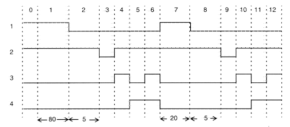
The implementation of the smart waveform generator is shown in the following example. It is similar to the waveform generator in the “Mealy Machine Schematic” figure in the Mealy Machine section, but has two additions. A new ROM, D_ROM, has been added to hold the length of each time step. A value of 1 specifies that the corresponding time step should be one clock cycle long; a value of 80 specifies that the time step should be 80 clock cycles long. The second addition to the previous waveform generator is a delay counter that counts the clock cycles between time steps.
In the architecture of the following example, a selected signal assignment determines the value of the NEXT_STEP counter.
package ROMS is
-- a 4x13 ROM called W_ROM containing the waveform

  constant W_ROM_WIDTH: INTEGER := 4;

  subtype W_ROM_WORD is BIT_VECTOR (1 to W_ROM_WIDTH);

  subtype W_ROM_RANGE is INTEGER range 0 to 12;

  type W_ROM_TABLE is array (0 to 12) of W_ROM_WORD;

  constant W_ROM: W_ROM_TABLE := W_ROM_TABLE'(

    ”1100”,   -- time step 0

    ”1100”,   -- time step 1

    ”0100”,   -- time step 2

    ”0000”,   -- time step 3

    ”0110”,   -- time step 4

    ”0101”,   -- time step 5

    ”0111”,   -- time step 6

    ”1100”,   -- time step 7

    ”0100”,   -- time step 8

    ”0000”,   -- time step 9

    ”0110”,   -- time step 10

    ”0101”,   -- time step 11

    ”0111”);  -- time step 12
  -- a 7x13 ROM called D_ROM containing the delays

  subtype D_ROM_WORD is INTEGER range 0 to 100;

  subtype D_ROM_RANGE is INTEGER range 0 to 12;

  type D_ROM_TABLE is array (0 to 12) of D_ROM_WORD;

  constant D_ROM: D_ROM_TABLE := D_ROM_TABLE'(

      1,80,5,1,1,1,1,20,5,1,1,1,1);

end ROMS;
use work.ROMS.all;

entity WAVEFORM is        -- Smart Waveform Generator

  port(CLOCK: in BIT;

       RESET: in BOOLEAN;

       WAVES: out W_ROM_WORD);

end WAVEFORM;
architecture BEHAVIOR of WAVEFORM is

  signal STEP, NEXT_STEP: W_ROM_RANGE;

  signal DELAY: D_ROM_WORD;

begin
  -- Determine the value of the next time step

  NEXT_STEP <= W_ROM_RANGE'high when

                    STEP = W_ROM_RANGE'high

               else

                 STEP + 1;

  -- Keep track of which time step we are in

  TIMESTEP_COUNTER: process

  begin

    wait until CLOCK'event and CLOCK = '1';

    if RESET then             -- Detect reset

      STEP <= 0;              -- Restart waveform

    elsif DELAY = 1 then

      STEP <= NEXT_STEP;      -- Continue stepping

    else

      null;          -- Wait for DELAY to count down;

    end if;          -- do nothing here

  end process TIMESTEP_COUNTER;
   -- Count the delay between time steps

  DELAY_COUNTER: process

  begin

    wait until CLOCK'event and CLOCK = '1';

    if RESET then             -- Detect reset

      DELAY <= D_ROM(0);      -- Restart

    elsif DELAY = 1 then      -- Have we counted down?

      DELAY <= D_ROM(NEXT_STEP);  -- Next delay value       else

      DELAY <= DELAY - 1;   -- decrement DELAY counter       end if;

    end process DELAY_COUNTER;
  WAVES <= W_ROM(STEP);     -- Output waveform value

end BEHAVIOR;
VHDL lets you create functions for use with array operands of any size. This example shows an adder-subtracter circuit that, when called, is adjusted to fit the size of its operands.
The following example shows an adder-subtracter defined for two unconstrained arrays of bits (type BIT_VECTOR) in a package named MATH. When an unconstrained array type is used for an argument to a subprogram, the actual constraints of the array are taken from the actual parameter values in a subprogram call.
package MATH is

  function ADD_SUB(L, R: BIT_VECTOR; ADD: BOOLEAN)

      return BIT_VECTOR;

    -- Add or subtract two BIT_VECTORs of equal length

end MATH;
package body MATH is

    function ADD_SUB(L, R: BIT_VECTOR; ADD: BOOLEAN)

        return BIT_VECTOR is

      variable CARRY: BIT;

      variable A, B, SUM:

          BIT_VECTOR(L'length-1 downto 0);

    begin

      if ADD then

          -- Prepare for an ”add” operation

          A := L;

          B := R;

          CARRY := '0';

      else
          -- Prepare for a ”subtract” operation

          A := L;

          B := not R;

          CARRY := '1';

      end if;
      -- Create a ripple carry chain; sum up bits

      for i in 0 to A'left loop

        SUM(i) := A(i) xor B(i) xor CARRY;

        CARRY := (A(i) and B(i)) or

                 (A(i) and CARRY) or

                 (CARRY and B(i));

      end loop;

      return SUM;        -- Result

    end;

end MATH;
Within the function ADD_SUB, two temporary variables, A and B, are declared. These variables are declared to be the same length as L (and necessarily, R) but have their index constraints normalized to L'length-1 downto 0. After the arguments are normalized, you can create a ripple carry adder by using a for loop.
No explicit references to a fixed array length are in the function ADD_SUB. Instead, the VHDL array attributes 'left and 'length are used. These attributes allow the function to work on arrays of any length.
The following example shows how to use the adder-subtracter defined in the MATH package. In this example, the vector arguments to functions ARG1 and ARG2 are declared as BIT_VECTOR(1 to 6). This declaration causes ADD_SUB to work with 6-bit arrays. A schematic of the synthesized circuit follows the example.
use work.MATH.all;
entity EXAMPLE is

    port(ARG1, ARG2: in BIT_VECTOR(1 to 6);

         ADD: in BOOLEAN;

         RESULT : out BIT_VECTOR(1 to 6));

end EXAMPLE;
architecture BEHAVIOR of EXAMPLE is

begin

  RESULT <= ADD_SUB(ARG1, ARG2, ADD);

end BEHAVIOR;
The count zeros - combinatorial example illustrates a design problem in which an 8-bit-wide value is given and the circuit determines two things.
The circuit produces two outputs: the number of zeros found and an error indication.
A valid input value can have at most one consecutive series of zeros. A value consisting entirely of ones is defined as a valid value. If a value is invalid, the zero counter resets to 0. For example, the value 00000000 is valid and has eight zeros; value 11000111 is valid and has three zeros; value 00111100 is invalid.
The following example shows the VHDL description for the circuit. It consists of a single process with a for loop that iterates across each bit in the given value. At each iteration, a temporary INTEGER variable (TEMP_COUNT) counts the number of zeros encountered. Two temporary Boolean variables (SEEN_ZERO and SEEN_TRAILING), initially false, are set to true when the beginning and end of the first sequence of zeros is detected.
If a zero is detected after the end of the first sequence of zeros (after SEEN_TRAILING is true), the zero count is reset (to 0), ERROR is set to true, and the for loop is exited.
The following example shows a combinatorial (parallel) approach to counting the zeros. The second example shows a sequential (serial) approach.
entity COUNT_COMB_VHDL is

  port(DATA:  in  BIT_VECTOR(7 downto 0);

       COUNT: out INTEGER range 0 to 8;

       ERROR: out BOOLEAN);

end COUNT_COMB_VHDL;
architecture BEHAVIOR of COUNT_COMB_VHDL is

begin

  process(DATA)

    variable TEMP_COUNT : INTEGER range 0 to 8;

    variable SEEN_ZERO, SEEN_TRAILING : BOOLEAN;

  begin

    ERROR <= FALSE;

    SEEN_ZERO <= FALSE;

    SEEN_TRAILING <= FALSE;

    TEMP_COUNT <= 0;

    for I in 0 to 7 loop

      if (SEEN_TRAILING and DATA(I) = '0') then

        TEMP_COUNT <= 0;

        ERROR <= TRUE;

        exit;

      elsif (SEEN_ZERO and DATA(I) = '1') then

        SEEN_TRAILING <= TRUE;

      elsif (DATA(I) = '0') then

        SEEN_ZERO <= TRUE;

        TEMP_COUNT <= TEMP_COUNT + 1;

      end if;

    end loop;
   COUNT <= TEMP_COUNT;

  end process;
end BEHAVIOR;
The count zeros - sequential example shows a sequential (clocked) variant of the preceding design (Count Zeros - Combinatorial Version).
The circuit now accepts the 8-bit data value serially, 1 bit per clock cycle, by using the DATA and CLK inputs. The other two inputs follow.
The circuit's three outputs follow.
Note: The output port COUNT is declared with mode BUFFER so that it can be read inside the process. OUT ports can only be written to, not read in.
entity COUNT_SEQ_VHDL is

  port(DATA, CLK: in BIT;

       RESET, READ: in BOOLEAN;

       COUNT: buffer INTEGER range 0 to 8;

       IS_LEGAL: out BOOLEAN;

       COUNT_READY: out BOOLEAN);

end COUNT_SEQ_VHDL;

architecture BEHAVIOR of COUNT_SEQ_VHDL is

begin

  process

    variable SEEN_ZERO, SEEN_TRAILING: BOOLEAN;

    variable BITS_SEEN: INTEGER range 0 to 7;

  begin

    wait until CLK'event and CLK = '1';
    if(RESET) then

      COUNT_READY<= FALSE;

      IS_LEGAL <= TRUE;-- signal assignment

      SEEN_ZERO<= FALSE;-- variable assignment

      SEEN_TRAILING <= FALSE;

      COUNT<= 0;

      BITS_SEEN<= 0;

    else

      if (READ) then

        if (SEEN_TRAILING and DATA = '0') then

          IS_LEGAL <= FALSE;

          COUNT <= 0;

          COUNT_READY <= TRUE;

        elsif (SEEN_ZERO and DATA = '1') then

          SEEN_TRAILING := TRUE;

        elsif (DATA = '0') then

          SEEN_ZERO <= TRUE;

          COUNT <= COUNT + 1;

        end if;
        if (BITS_SEEN = 7) then

          COUNT_READY <= TRUE;

        else

          BITS_SEEN <=  BITS_SEEN + 1;

        end if;
      end if;    -- if (READ)

    end if;      -- if (RESET)

  end process;

end BEHAVIOR;
The soft drink machine - state machine example is a control unit for a soft drink vending machine.
The circuit reads signals from a coin input unit and sends outputs to a change dispensing unit and a drink dispensing unit.
Here are the design parameters for the following two examples.
library synopsys; use synopsys.attributes.all;
entity DRINK_STATE_VHDL is

  port(NICKEL_IN, DIME_IN, QUARTER_IN, RESET: BOOLEAN;

       CLK: BIT;

       NICKEL_OUT, DIME_OUT, DISPENSE: out BOOLEAN);

end DRINK_STATE_VHDL;
architecture BEHAVIOR of DRINK_STATE_VHDL is

  type STATE_TYPE is (IDLE, FIVE, TEN, FIFTEEN,             TWENTY, TWENTY_FIVE, THIRTY, OWE_DIME);

  signal CURRENT_STATE, NEXT_STATE: STATE_TYPE;

  attribute STATE_VECTOR : STRING;

  attribute STATE_VECTOR of BEHAVIOR : architecture is

 ”CURRENT_STATE”;
attribute sync_set_reset of reset : signal is ”true”;

begin
   process(NICKEL_IN, DIME_IN, QUARTER_IN,

          CURRENT_STATE, RESET, CLK)

  begin

    -- Default assignments

    NEXT_STATE <= CURRENT_STATE;

    NICKEL_OUT <= FALSE;

    DIME_OUT <= FALSE;

    DISPENSE <= FALSE;
    -- Synchronous reset

    if(RESET) then

      NEXT_STATE <= IDLE;

    else
    -- State transitions and output logic

    case CURRENT_STATE is

        when IDLE =>

          if(NICKEL_IN) then

            NEXT_STATE <= FIVE;

          elsif(DIME_IN) then

            NEXT_STATE <= TEN;

          elsif(QUARTER_IN) then

            NEXT_STATE <= TWENTY_FIVE;

          end if;
        when FIVE =>

          if(NICKEL_IN) then

            NEXT_STATE <= TEN;

          elsif(DIME_IN) then

            NEXT_STATE <= FIFTEEN;

          elsif(QUARTER_IN) then

            NEXT_STATE <= THIRTY;

          end if;

        when TEN =>

          if(NICKEL_IN) then

            NEXT_STATE <= FIFTEEN;

          elsif(DIME_IN) then

            NEXT_STATE <= TWENTY;

          elsif(QUARTER_IN) then

            NEXT_STATE <= IDLE;

            DISPENSE <= TRUE;

          end if;

        when FIFTEEN =>

          if(NICKEL_IN) then

            NEXT_STATE <= TWENTY;

          elsif(DIME_IN) then

            NEXT_STATE <= TWENTY_FIVE;

          elsif(QUARTER_IN) then

            NEXT_STATE <= IDLE;

            DISPENSE <= TRUE;

            NICKEL_OUT <= TRUE;

          end if;

        when TWENTY =>

          if(NICKEL_IN) then

            NEXT_STATE <= TWENTY_FIVE;

          elsif(DIME_IN) then

            NEXT_STATE <= THIRTY;

          elsif(QUARTER_IN) then

            NEXT_STATE <= IDLE;

            DISPENSE <= TRUE;

            DIME_OUT <= TRUE;

          end if;
when TWENTY_FIVE =>

          if(NICKEL_IN) then

            NEXT_STATE <= THIRTY;

          elsif(DIME_IN) then

            NEXT_STATE <= IDLE;

            DISPENSE <= TRUE;

          elsif(QUARTER_IN) then

            NEXT_STATE <= IDLE;

            DISPENSE <= TRUE;

            DIME_OUT <= TRUE;

            NICKEL_OUT <= TRUE;

          end if;
        when THIRTY =>

          if(NICKEL_IN) then

            NEXT_STATE <= IDLE;

            DISPENSE <= TRUE;

          elsif(DIME_IN) then

            NEXT_STATE <= IDLE;

            DISPENSE <= TRUE;

            NICKEL_OUT <= TRUE;

          elsif(QUARTER_IN) then

            NEXT_STATE <= OWE_DIME;

            DISPENSE <= TRUE;

            DIME_OUT <= TRUE;

          end if;
        when OWE_DIME =>

          NEXT_STATE <= IDLE;

          DIME_OUT <= TRUE;
      end case;

    end if;

  end process;
  -- Synchronize state value with clock

  -- This causes it to be stored in flip-flops

  process

  begin

    wait until CLK'event and CLK = '1';

    CURRENT_STATE <= NEXT_STATE;

  end process;

end BEHAVIOR;
The soft drink machine - count nickels example uses the same design parameters as the preceding example of a soft drink machine - state machine with the same input and output signals. In this version, a counter counts the number of nickels deposited. The counter in the following example is incremented by one if the deposit is a nickel, by two if it is a dime, and by five if it is a quarter.
entity DRINK_COUNT_VHDL is

  port(NICKEL_IN, DIME_IN, QUARTER_IN, RESET:             BOOLEAN;

       CLK: BIT;

       NICKEL_OUT, DIME_OUT, DISPENSE: out BOOLEAN);

end DRINK_COUNT_VHDL;
architecture BEHAVIOR of DRINK_COUNT_VHDL is

  signal CURRENT_NICKEL_COUNT,

         NEXT_NICKEL_COUNT: INTEGER range 0 to 7;

  signal CURRENT_RETURN_CHANGE, NEXT_RETURN_CHANGE : BOOLEAN;

begin
process(NICKEL_IN, DIME_IN, QUARTER_IN, RESET, CLK,

          CURRENT_NICKEL_COUNT, CURRENT_RETURN_CHANGE)

    variable TEMP_NICKEL_COUNT: INTEGER range 0 to 12;

begin

    -- Default assignments

    NICKEL_OUT <= FALSE;

    DIME_OUT <= FALSE;

    DISPENSE <= FALSE;

    NEXT_NICKEL_COUNT <= 0;

    NEXT_RETURN_CHANGE <= FALSE;
-- Synchronous reset

    if (not RESET) then

      TEMP_NICKEL_COUNT <= CURRENT_NICKEL_COUNT;
      -- Check whether money has come in

      if (NICKEL_IN) then

        -- NOTE:  This design will be flattened, so

        --   these multiple adders will be optimized

        TEMP_NICKEL_COUNT <= TEMP_NICKEL_COUNT + 1;

      elsif(DIME_IN) then

        TEMP_NICKEL_COUNT <= TEMP_NICKEL_COUNT + 2;

      elsif(QUARTER_IN) then

        TEMP_NICKEL_COUNT <= TEMP_NICKEL_COUNT + 5;

      end if;
      -- Enough deposited so far?

      if(TEMP_NICKEL_COUNT >= 7) then

        TEMP_NICKEL_COUNT <= TEMP_NICKEL_COUNT - 7;

        DISPENSE <= TRUE;

      end if;
      -- Return change

      if(TEMP_NICKEL_COUNT >= 1 or

         CURRENT_RETURN_CHANGE) then

        if(TEMP_NICKEL_COUNT >= 2) then

          DIME_OUT <= TRUE;

          TEMP_NICKEL_COUNT <= TEMP_NICKEL_COUNT - 2;

          NEXT_RETURN_CHANGE <= TRUE;

        end if;

        if(TEMP_NICKEL_COUNT = 1) then

          NICKEL_OUT <= TRUE;

          TEMP_NICKEL_COUNT <= TEMP_NICKEL_COUNT - 1;

        end if;

      end if;
       NEXT_NICKEL_COUNT <= TEMP_NICKEL_COUNT;

    end if;

  end process;
  -- Remember the return-change flag and

  -- the nickel count for the next cycle

  process

  begin

    wait until CLK'event and CLK = '1';

    CURRENT_RETURN_CHANGE <= NEXT_RETURN_CHANGE;

    CURRENT_NICKEL_COUNT <= NEXT_NICKEL_COUNT;

  end process;
end BEHAVIOR;
This example of a carry-lookahead adder uses concurrent procedure calls to build a 32-bit carry-lookahead adder. The adder is built by partitioning of the 32-bit input into eight slices of 4 bits each. Each of the eight slices computes propagate and generate values by using the PG procedure.
Propagate (output P from PG) is '1' for a bit position if that position propagates a carry from the next-lower position to the next-higher position. Generate (output G) is '1' for a bit position if that position generates a carry to the next-higher position, regardless of the carry-in from the next lower position. The carry-lookahead logic reads the carry-in, propagate, and generate information computed from the inputs. The logic computes the carry value for each bit position and makes the addition operation an XOR of the inputs and the carry values.
The carry values are computed by a three-level tree of 4-bit carry-lookahead blocks.
The VHDL implementation of the design in the previous figure is accomplished with four procedures:
The following example shows a VHDL description of the adder.
package LOCAL is

   constant N:    INTEGER := 4;
procedure BITSLICE(

      A, B: in BIT_VECTOR(3 downto 0);

      CIN: in BIT;

      signal S: out BIT_VECTOR(3 downto 0);

      signal GP, GG: out BIT);

  procedure PG(

      A, B: in BIT_VECTOR(3 downto 0);

      P, G: out BIT_VECTOR(3 downto 0));

  function SUM(A, B, C: BIT_VECTOR(3 downto 0))

      return BIT_VECTOR;

  procedure CLA(

      P, G: in BIT_VECTOR(3 downto 0);

      CIN: in BIT;

      C: out BIT_VECTOR(3 downto 0);

      signal GP, GG: out BIT);

end LOCAL;
package body LOCAL is

  -----------------------------------------------

  -- Compute sum and group outputs from a, b, cin

  -----------------------------------------------

procedure BITSLICE(

      A, B: in BIT_VECTOR(3 downto 0);

      CIN: in BIT;

      signal S: out BIT_VECTOR(3 downto 0);

      signal GP, GG: out BIT) is
    variable P, G, C: BIT_VECTOR(3 downto 0);

  begin

    PG(A, B, P, G);

    CLA(P, G, CIN, C, GP, GG);

    S <= SUM(A, B, C);

  end;
----------------------------------------------------

  -- Compute propagate and generate from input bits

----------------------------------------------------
procedure PG(A, B: in BIT_VECTOR(3 downto 0);

               P, G: out BIT_VECTOR(3 downto 0)) is
begin

    P <= A or B;

    G <= A and B;

end;
----------------------------------------------------

  -- Compute sum from the input bits and the carries

----------------------------------------------------
function SUM(A, B, C: BIT_VECTOR(3 downto 0))

      return BIT_VECTOR is
begin

    return(A xor B xor C);

  end;
--------------------------------

  -- 4-bit carry-lookahead block

--------------------------------
procedure CLA(

      P, G: in BIT_VECTOR(3 downto 0);

      CIN: in BIT;

      C: out BIT_VECTOR(3 downto 0);

      signal GP, GG: out BIT) is

    variable TEMP_GP, TEMP_GG, LAST_C: BIT;

begin

    TEMP_GP <= P(0);

    TEMP_GG <= G(0);

    LAST_C <= CIN;

    C(0) <= CIN;
    for I in 1 to N-1 loop

      TEMP_GP <= TEMP_GP and P(I);

      TEMP_GG <= (TEMP_GG and P(I)) or G(I);

      LAST_C <= (LAST_C and P(I-1)) or G(I-1);

      C(I) <= LAST_C;

    end loop;
    GP <= TEMP_GP;

    GG <= TEMP_GG;

  end;

end LOCAL;
use WORK.LOCAL.ALL;
---------------------------------

-- A 32-bit carry-lookahead adder

---------------------------------
entity ADDER is

  port(A, B: in BIT_VECTOR(31 downto 0);

       CIN: in BIT;

       S: out BIT_VECTOR(31 downto 0);

       COUT: out BIT);

end ADDER;

architecture BEHAVIOR of ADDER is
  signal GG,GP,GC: BIT_VECTOR(7 downto 0);

    -- First-level generate, propagate, carry

  signal GGG, GGP, GGC: BIT_VECTOR(3 downto 0);

    -- Second-level gen, prop, carry

  signal GGGG, GGGP: BIT;

    -- Third-level gen, prop
begin

  -- Compute Sum and 1st-level Generate and Propagate

  -- Use input data and the 1st-level Carries computed

  -- later.

  BITSLICE(A( 3 downto  0),B( 3 downto  0),GC(0),

           S( 3 downto  0),GP(0), GG(0));

  BITSLICE(A( 7 downto  4),B( 7 downto  4),GC(1),

           S( 7 downto  4),GP(1), GG(1));

  BITSLICE(A(11 downto  8),B(11 downto  8),GC(2),

           S(11 downto  8),GP(2), GG(2));

  BITSLICE(A(15 downto 12),B(15 downto 12),GC(3),

           S(15 downto 12),GP(3), GG(3));

  BITSLICE(A(19 downto 16),B(19 downto 16),GC(4),

           S(19 downto 16),GP(4), GG(4));

  BITSLICE(A(23 downto 20),B(23 downto 20),GC(5),

           S(23 downto 20),GP(5), GG(5));

  BITSLICE(A(27 downto 24),B(27 downto 24),GC(6),

           S(27 downto 24),GP(6), GG(6));

  BITSLICE(A(31 downto 28),B(31 downto 28),GC(7),

           S(31 downto 28),GP(7), GG(7));
  -- Compute first-level Carries and second-level

  -- generate and propagate.

  -- Use first-level Generate, Propagate, and

  -- second-level carry.

  process(GP, GG, GGC)

    variable TEMP: BIT_VECTOR(3 downto 0);

  begin

    CLA(GP(3 downto 0), GG(3 downto 0), GGC(0), TEMP,

        GGP(0), GGG(0));

    GC(3 downto 0) <= TEMP;

  end process;
process(GP, GG, GGC)

    variable TEMP: BIT_VECTOR(3 downto 0);

  begin

    CLA(GP(7 downto 4), GG(7 downto 4), GGC(1), TEMP,

        GGP(1), GGG(1));

    GC(7 downto 4) <= TEMP;

  end process;
  -- Compute second-level Carry and third-level

  --   Generate and Propagate

  -- Use second-level Generate, Propagate and Carry-in

  --   (CIN)

  process(GGP, GGG, CIN)

    variable TEMP: BIT_VECTOR(3 downto 0);

  begin

    CLA(GGP, GGG, CIN, TEMP, GGGP, GGGG);

    GGC <= TEMP;

  end process;
  -- Assign unused bits of second-level Generate and

  --   Propagate

  GGP(3 downto 2) <= ”11”;

  GGG(3 downto 2) <= ”00”;
  -- Compute Carry-out (COUT)

  -- Use third-level Generate and Propagate and

  --   Carry-in (CIN).

  COUT <= GGGG or (GGGP and CIN);

end BEHAVIOR;
In the carry-lookahead adder implementation, procedures perform the computation of the design. The procedures can also be in the form of separate entities and used by component instantiation, producing a hierarchical design. Foundation Express does not collapse a hierarchy of entities, but it does collapse the procedure call hierarchy into one design.
The keyword signal is included before some of the interface parameter declarations. This keyword is required for the out formal parameters when the actual parameters must be signals.
The output parameter C from the CLA procedure is not declared as a signal; thus, it is not allowed in a concurrent procedure call. Only signals can be used in such calls. To overcome this problem, subprocesses are used, declaring a temporary variable TEMP. TEMP receives the value of the C parameter and assigns it to the appropriate signal (a generally useful technique).
This example shows the design of a serial-to-parallel converter that reads a serial, bit-stream input and produces an 8-bit output.
The design reads the following inputs.
The design produces the following outputs:
When no data is being transmitted to the serial port, keep it at a value of '0'. Each 8-bit value requires ten clock cycles to read it. On the eleventh clock cycle, the parallel output value can be read.
In the first cycle, a '1' is placed on the serial input. This assignment indicates that an 8-bit value follows. The next eight cycles transmit each bit of the value. The most significant bit is transmitted first. The tenth cycle transmits the parity of the 8-bit value. It must be '0' if an even number of '1' values are in the 8-bit data, and '1' otherwise. If the converter detects a parity error, it sets the PARITY_ERROR output to '1' and waits until the value is reset.
On the eleventh cycle, the READ_ENABLE output is set to '1' and the 8-bit value can be read from the PARALLEL_OUT port. If the SERIAL_IN port has a '1' on the eleventh cycle, another 8-bit value is read immediately; otherwise, the converter waits until SERIAL_IN goes to '1'.
The following figure shows the timing of this design.
The implementation of the converter is as a four-state finite-state machine with synchronous reset. When a reset is detected, the converter enters a WAIT_FOR_START state. The description of each state follows.
This design has four values stored in registers.
The design has two processes: the combinatorial NEXT_ST containing the combinatorial logic and the sequential SYNCH that is clocked.
NEXT_ST performs all the computations and state assignments. The NEXT_ST process starts by assigning default values to all the signals it drives. This assignment guarantees that all signals are driven under all conditions. Next, the RESET input is processed. If RESET is not active, a case statement determines the current state and its computations. State transitions are performed by assigning the next state's value you want to the NEXT_STATE signal.
The serial-to-parallel conversion itself is performed by these two statements in the NEXT_ST process.
NEXT_PARALLEL_OUT(CURRENT_BIT_POSITION) <= SERIAL_IN;

NEXT_BIT_POSITION <= CURRENT_BIT_POSITION + 1;
The first statement assigns the current serial input bit to a particular bit of the parallel output. The second statement increments the next bit position to be assigned.
SYNCH registers and updates the stored values previously described. Each registered signal has two parts, NEXT_... and CURRENT_... :
The following example shows a VHDL description of the converter.
-- Serial-to-Parallel Converter, counting bits
package TYPES is

  -- Declares types used in the rest of the design

  type STATE_TYPE is (WAIT_FOR_START,

                      READ_BITS,

                      PARITY_ERROR_DETECTED,

                      ALLOW_READ);

  constant PARALLEL_BIT_COUNT: INTEGER := 8;

  subtype PARALLEL_RANGE is INTEGER

      range 0 to (PARALLEL_BIT_COUNT-1);

  subtype PARALLEL_TYPE is BIT_VECTOR(PARALLEL_RANGE);

end TYPES;
use WORK.TYPES.ALL; -- Use the TYPES package
entity SER_PAR is       -- Declare the interface

  port(SERIAL_IN, CLOCK, RESET: in BIT;

       PARALLEL_OUT: out PARALLEL_TYPE;

       PARITY_ERROR, READ_ENABLE: out BIT);

end SER_PAR;
architecture BEHAVIOR of SER_PAR is

  -- Signals for stored values

  signal CURRENT_STATE, NEXT_STATE: STATE_TYPE;

  signal CURRENT_PARITY, NEXT_PARITY: BIT;

  signal CURRENT_BIT_POSITION, NEXT_BIT_POSITION:

      INTEGER range PARALLEL_BIT_COUNT downto 0;

  signal CURRENT_PARALLEL_OUT, NEXT_PARALLEL_OUT:

      PARALLEL_TYPE;

begin

NEXT_ST: process(SERIAL_IN, CURRENT_STATE, RESET,

                 CURRENT_BIT_POSITION, CURRENT_PARITY,

                 CURRENT_PARALLEL_OUT)

  -- This process computes all outputs, the next

  --   state, and the next value of all stored values

  begin

    PARITY_ERROR <= '0'; -- Default values for all

    READ_ENABLE <= '0';  --  outputs and stored values

    NEXT_STATE <= CURRENT_STATE;

    NEXT_BIT_POSITION <= 0;

    NEXT_PARITY <= '0';

    NEXT_PARALLEL_OUT <= CURRENT_PARALLEL_OUT;
if (RESET = '1') then      -- Synchronous reset

      NEXT_STATE <= WAIT_FOR_START;

    else

      case CURRENT_STATE is   -- State processing

        when WAIT_FOR_START =>

          if (SERIAL_IN = '1') then

            NEXT_STATE <= READ_BITS;

            NEXT_PARALLEL_OUT <=

                PARALLEL_TYPE'(others=>'0');

          end if;

        when READ_BITS =>

          if (CURRENT_BIT_POSITION =

              PARALLEL_BIT_COUNT) then

            if (CURRENT_PARITY = SERIAL_IN) then

              NEXT_STATE <= ALLOW_READ;

              READ_ENABLE <= '1';

            else

              NEXT_STATE <= PARITY_ERROR_DETECTED;

            end if;

          else

            NEXT_PARALLEL_OUT(CURRENT_BIT_POSITION) <=

                SERIAL_IN;

            NEXT_BIT_POSITION <=

                CURRENT_BIT_POSITION + 1;

            NEXT_PARITY <= CURRENT_PARITY xor

                           SERIAL_IN;

          end if;

        when PARITY_ERROR_DETECTED =>

          PARITY_ERROR <= '1';

        when ALLOW_READ =>

          NEXT_STATE <= WAIT_FOR_START;

      end case;

    end if;

  end process NEXT_ST;
SYNCH: process

    -- This process remembers the stored values

    --    across clock cycles

begin

    wait until CLOCK'event and CLOCK = '1';

    CURRENT_STATE <= NEXT_STATE;

    CURRENT_BIT_POSITION <= NEXT_BIT_POSITION;

    CURRENT_PARITY <= NEXT_PARITY;

    CURRENT_PARALLEL_OUT <= NEXT_PARALLEL_OUT;

end process SYNCH;
PARALLEL_OUT <= CURRENT_PARALLEL_OUT;
end BEHAVIOR;
This example describes another implementation of the serial-to-parallel converter in the last example. This design performs the same function as the previous one but uses a different algorithm to do the conversion.
The previous implementation used a counter to indicate the bit of the output that was set when a new serial bit was read. In this implementation, the serial bits are shifted into place. Before the conversion occurs, a '1' is placed in the least-significant bit position. When that '1' is shifted out of the most significant position (position 0), the signal NEXT_HIGH_BIT is set to '1' and the conversion is complete.
The following example shows the listing of the second implementation. The differences are highlighted in bold. The differences relate to the removal of the ..._BIT_POSITION signals, the addition of ..._HIGH_BIT signals, and the change in the way NEXT_PARALLEL_OUT is computed.
package TYPES is

  -- Declares types used in the rest of the design

  type STATE_TYPE is (WAIT_FOR_START,

                      READ_BITS,

                      PARITY_ERROR_DETECTED,

                      ALLOW_READ);

  constant PARALLEL_BIT_COUNT: INTEGER := 8;

  subtype PARALLEL_RANGE is INTEGER

      range 0 to (PARALLEL_BIT_COUNT-1);

  subtype PARALLEL_TYPE is            BIT_VECTOR(PARALLEL_RANGE);

end TYPES;
use WORK.TYPES.ALL; -- Use the TYPES package
entity SER_PAR is        -- Declare the interface

  port(SERIAL_IN, CLOCK, RESET: in BIT;

       PARALLEL_OUT: out PARALLEL_TYPE;

       PARITY_ERROR, READ_ENABLE: out BIT);

end SER_PAR;
architecture BEHAVIOR of SER_PAR is

  -- Signals for stored values

  signal CURRENT_STATE, NEXT_STATE: STATE_TYPE;
  signal CURRENT_PARITY, NEXT_PARITY: BIT;

  signal CURRENT_HIGH_BIT, NEXT_HIGH_BIT: BIT;

  signal CURRENT_PARALLEL_OUT, NEXT_PARALLEL_OUT:

     PARALLEL_TYPE;

begin
NEXT_ST: process(SERIAL_IN, CURRENT_STATE, RESET,

                 CURRENT_HIGH_BIT, CURRENT_PARITY,

                 CURRENT_PARALLEL_OUT)

  -- This process computes all outputs, the next

  --   state, and the next value of all stored values

  begin

    PARITY_ERROR <= '0'; -- Default values for all

    READ_ENABLE <= '0';  --  outputs and stored values

    NEXT_STATE <= CURRENT_STATE;

    NEXT_HIGH_BIT <= '0';

    NEXT_PARITY <= '0';

    NEXT_PARALLEL_OUT <= PARALLEL_TYPE'(others=>'0');

    if(RESET = '1') then      -- Synchronous reset

      NEXT_STATE <= WAIT_FOR_START;

    else

      case CURRENT_STATE is   -- State processing

        when WAIT_FOR_START =>

          if (SERIAL_IN = '1') then

            NEXT_STATE <= READ_BITS;

            NEXT_PARALLEL_OUT <=

                PARALLEL_TYPE'(others=>'0');

          end if;

        when READ_BITS =>

          if (CURRENT_HIGH_BIT = '1') then

            if (CURRENT_PARITY = SERIAL_IN) then

              NEXT_STATE <= ALLOW_READ;

              READ_ENABLE <= '1';

            else

              NEXT_STATE <= PARITY_ERROR_DETECTED;

            end if;

          else

            NEXT_HIGH_BIT <= CURRENT_PARALLEL_OUT(0);

            NEXT_PARALLEL_OUT <=

                CURRENT_PARALLEL_OUT(

                    1 to PARALLEL_BIT_COUNT-1) &

                SERIAL_IN;

            NEXT_PARITY <= CURRENT_PARITY xor

                           SERIAL_IN;

          end if;

        when PARITY_ERROR_DETECTED =>

          PARITY_ERROR <= '1';

        when ALLOW_READ =>

          NEXT_STATE <= WAIT_FOR_START;

      end case;

    end if;

  end process NEXT_ST;
  SYNCH: process

    -- This process remembers the stored values

    --    across clock cycles

  begin

    wait until CLOCK'event and CLOCK = '1';

    CURRENT_STATE <= NEXT_STATE;

    CURRENT_HIGH_BIT <= NEXT_HIGH_BIT;

    CURRENT_PARITY <= NEXT_PARITY;

    CURRENT_PARALLEL_OUT <= NEXT_PARALLEL_OUT;

  end process SYNCH;
PARALLEL_OUT <= CURRENT_PARALLEL_OUT;
end BEHAVIOR;
Note: The synthesized schematic for the shifter implementation is much simpler than that of the previous count implementation in the example of the serial-to-parallel converter - counting bits. It is simpler because the shifter algorithm is inherently easier to implement.
With the count algorithm, each of the flip-flops holding the PARALLEL_OUT bits needed logic that decoded the value stored in the BIT_POSITION flip-flops to see when to route in the value of SERIAL_IN. Also, the BIT_POSITION flip-flops needed an incrementer to compute their next value.
In contrast, the shifter algorithm requires neither an incrementer nor flip-flops to hold BIT_POSITION. Additionally, the logic in front of most PARALLEL_OUT bits needs to read only the value of the previous flip-flop or '0'. The value depends on whether bits are currently being read. In the shifter algorithm, the SERIAL_IN port needs to be connected only to the least significant bit (number 7) of the PARALLEL_OUT flip-flops.
These two implementations illustrate the importance of designing efficient algorithms. Both work properly, but the shifter algorithm produces a faster, more area-efficient design.
This example shows a way to build programmable logic arrays (PLAs) in VHDL. The PLA function uses an input lookup vector as an index into a constant PLA table and then returns the output vector specified by the PLA.
The PLA table is an array of PLA rows, where each row is an array of PLA elements. Each element is either a one, a zero, a minus, or a space ('1', '0', '-', or ' '). The table is split between an input plane and an output plane. The input plane is specified by zeros, ones, and minuses. The output plane is specified by zeros and ones. The two planes' values are separated by a space.
In the PLA function, the output vector is first initialized to be all zeros. When the input vector matches an input plane in a row of the PLA table, the ones in the output plane are assigned to the corresponding bits in the output vector. A match is determined as follows.
The generic PLA table types and the PLA function are defined in a package named LOCAL. An entity PLA_VHDL that uses LOCAL needs only to specify its PLA table as a constant, then call the PLA function.
The PLA function does not explicitly depend on the size of the PLA. To change the size of the PLA, change the initialization of the TABLE constant and the initialization of the constants INPUT_COUNT, OUTPUT_COUNT, and ROW_COUNT. In the following example, these constants are initialized to a PLA equivalent to the ROM shown previously in the ROM example in the “Read-Only Memory” section of this appendix. Accordingly, the synthesized schematic is the same as that of the ROM, with one difference: in the example of the implementation of a ROM in random logic, the DATA output port range is 1 to 5; in the following example, the OUT_VECTOR output port range is 4 down to 0.
package LOCAL is

  constant INPUT_COUNT: INTEGER := 3;

  constant OUTPUT_COUNT: INTEGER := 5;

  constant ROW_COUNT: INTEGER := 6;

  constant ROW_SIZE: INTEGER := INPUT_COUNT +

                                OUTPUT_COUNT + 1;

  type PLA_ELEMENT is ('1', '0', '-', ' ');

  type PLA_VECTOR is

      array (INTEGER range <>) of PLA_ELEMENT;

  subtype PLA_ROW is

      PLA_VECTOR(ROW_SIZE - 1 downto 0);

  subtype PLA_OUTPUT is

      PLA_VECTOR(OUTPUT_COUNT - 1 downto 0);

  type PLA_TABLE is

      array(ROW_COUNT - 1 downto 0) of PLA_ROW;
  function PLA(IN_VECTOR: BIT_VECTOR;

               TABLE: PLA_TABLE)

      return BIT_VECTOR;

end LOCAL;
package body LOCAL is
   function PLA(IN_VECTOR: BIT_VECTOR;

               TABLE: PLA_TABLE)

      return BIT_VECTOR is

    subtype RESULT_TYPE is

        BIT_VECTOR(OUTPUT_COUNT - 1 downto 0);

    variable RESULT: RESULT_TYPE;

    variable ROW: PLA_ROW;

    variable MATCH: BOOLEAN;

    variable IN_POS: INTEGER;
   begin

    RESULT <= RESULT_TYPE'(others => BIT'( '0' ));

    for I in TABLE'range loop

      ROW <= TABLE(I);

      MATCH <= TRUE;

      IN_POS <= IN_VECTOR'left;
      -- Check for match in input plane

      for J in ROW_SIZE - 1 downto OUTPUT_COUNT loop

        if(ROW(J) = PLA_ELEMENT'( '1' )) then

          MATCH <= MATCH and

                   (IN_VECTOR(IN_POS) = BIT'( '1' ));

        elsif(ROW(J) = PLA_ELEMENT'( '0' )) then

          MATCH <= MATCH and

                   (IN_VECTOR(IN_POS) = BIT'( '0' ));

        else

          null;     -- Must be minus (”don't care”)

        end if;

        IN_POS <= IN_POS - 1;

      end loop;
      -- Set output plane

      if(MATCH) then

        for J in RESULT'range loop

          if(ROW(J) = PLA_ELEMENT'( '1' )) then

            RESULT(J) <= BIT'( '1' );

          end if;

        end loop;

      end if;

    end loop;

    return(RESULT);

  end;

end LOCAL;
use WORK.LOCAL.all;

entity PLA_VHDL is

  port(IN_VECTOR: BIT_VECTOR(2 downto 0);

       OUT_VECTOR: out BIT_VECTOR(4 downto 0));

end PLA_VHDL;
architecture BEHAVIOR of PLA_VHDL is

  constant TABLE: PLA_TABLE := PLA_TABLE'(

       PLA_ROW'(”--- 10000”),

       PLA_ROW'(”-1- 01000”),

       PLA_ROW'(”0-0 00101”),

       PLA_ROW'(”-1- 00101”),

       PLA_ROW'(”1-1 00101”),

       PLA_ROW'(”-1- 00010”));
begin

  OUT_VECTOR <= PLA(IN_VECTOR, TABLE);

end BEHAVIOR;